This is the story of how I daisy-chained a bunch of electronic shelf labels (ESL) to decorate my office wall.
A few months ago, I came across @atc1441’s work on reverse engineering one of these ESLs. I found a box with 25 of them on eBay for $35 and joined the party.
They pack a similar brain as a fitness tracker I poked. I played with them for a couple of hours and even contributed an implementation of a Bluetooth Low Energy (BLE) service that lets you draw stuff on them wirelessly. It was fun, but that was the end of my short stunt with the labels.
It was not until months later that I stumbled upon @scottbez1’s excellent video “How a Split-Flap Display Works” and had the idea of linking a bunch of small e-paper displays together in a similar fashion. I dusted off the box with the ESLs and got to work.
The Setup
In the wild, these displays are usually controlled with a purpose-built device that talks to them via RF or NFC. This video shows NFC in action.
The particular SoC in the ESLs I have, the TLSR8359, is additionally BLE-capable. The documentation is not very explicit about it, but it’s there.
In theory, you can just line up a bunch of them and sequentially connect to one after the other via BLE, push some data, draw it and move on. This would have been a lot easier, as most of the BLE stuff was already implemented.
I chose a different route, in which only the first ESL is connectable via BLE and all nodes are physically connected via their UART pins:
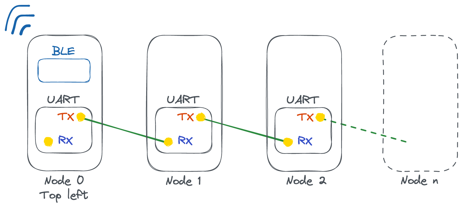 Figure 1. A bunch of ESLs chained together via their UART ports
There are two small advantages and one big one to this approach:
- It’s a lot faster to connect to a single BLE device and push all the data than it is to connect to 20 devices, specially if they keep their advertisement interval to a minimum to save battery;
- Only one device has its radio on. All other devices can deep sleep even deeper, lowering their individual current consumption by an order of magnitude;
- It seemed like a lot of fun to design and implement a message-relaying protocol over UART, similarly to a ring network.
The Protocol
Each node runs the following algorithm:
Run forever:
  message := read_incoming_message()
  if (message is for me):
    process_message(message)
  else:
    send_to_next_node_via_uart(message)
Listing 1: Simplified algorithm
An important part is that every node (except the first, that has BLE turned on) is running the exact same firmware - you could swap any two of them and everything would work exactly the same. This is by design - I didn’t want to build the code 20 times with different parameters.
So how does a node know when a message is for them? Here’s how a message is implemented in the real firmware (edited for brevity):
typedef struct {
  // Number of hops this message needs to take.
  uint8_t hops;
  // Operation to perform.
  uint8_t op;
  uint16_t data_len;
} elink_packet_header_t;

typedef struct {
  elink_packet_header_t header;
  // Data. Its meaning depends on the header.op.
  uint8_t data[ELINK_BUF_SIZE];
} elink_packet_t;
Listing 2. elink_packet_t represents a message flowing through the array
When a node receives an elink_packet_t, it inspects its header.hops field. If it’s 0, then the message is for the current node. If it’s nonzero, the current node decrements its value and forwards the whole message to the next node.
A nice convenience is that this protocol layer is transport-agnostic. The first node can receive messages from BLE or from UART. In the Python client we will see next, you can simply specify --transport=ble or --transport=uart when pushing data to the array, and everything else remains the same.
Operations
Different features are implemented as different operations. They instruct nodes about what to do, and are carried in the op field of the elink_packet_header_t struct. Some operations are:
- Clear the screen
- Write an image to the screen
- Render a character with a given font and draw it on the screen
- Render a string with a given font and
(y, x)location and draw it on the screen - Toggle the built-in LED - useful for debugging
- Go to deep sleep
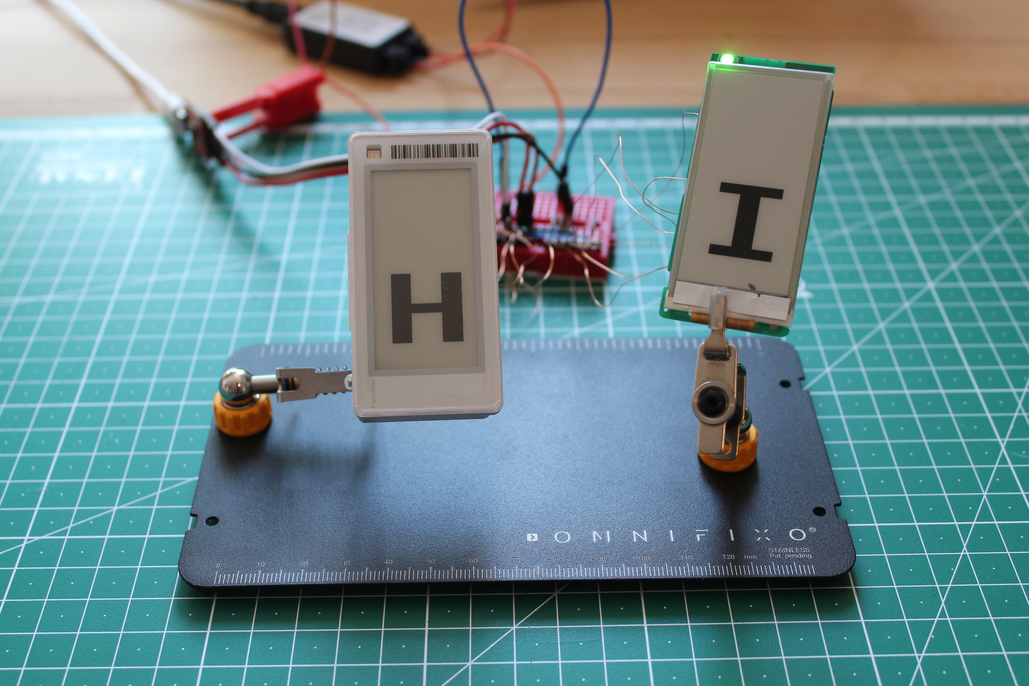 Figure 2. The first prototype
Power Management
Each Coulomb of charge is at a premium in these tiny-battery-operated devices. I have dipped my toes in a couple of ultra-low-power hobby projects, but it’s still hard to grasp how efficient this SoCs can be.
The main trick these chips use is to spend most of the time in a very low-power state, known as deep sleep. This is an incredible world on its own. There are many different types and tradeoffs between sleeping modes, and different chip manufactures offer some variations of them.
To wake up the CPU back to life, usual choices are:
- A timer, in which case the SoC needs to keep tabs of time while sleeping
- A change in the logic state on one of its input pins
Option 1 is good for periodic tasks, like taking a quick reading of a sensor and going right back to sleep. Option 2 is good for responding to some external events, like a door closing, an NFC tag approaching or, in our case, a new message arriving.
I had to reuse the same RX-TX connection as a wake-up source for two reasons:
- There were no more GPIOs exposed as test pads in the back of the ESLs
- Avoiding having to solder another run of wire
In this fashion, right before going to sleep, each node will reconfigure its RX pin to serve as a wake-up source. As a side effect, whenever the previous node wakes up and immediately sets up its UART module, there’s enough of a blip in the line that wakes up the next node, and so on and so forth until all nodes are brought back to life.
Alternative Idea
Another valid approach is elect a coordinator and make it responsible for completely cutting off and restoring power to the rest of the array. This yields lower overall deep-sleep current, as most of the devices are truly disconnected from power. The downside is that we need extra circuitry and we lose the ability of progressively sending nodes to sleep once their work is done - it’s all or nothing.
BLE Node
Low-power BLE devices have an extra concern. While they need to save as much juice as possible, they also want to, at the very least, broadcast their existence (with possibly some attached data). Some BLE devices, like these ESLs, are also connectable, which means they periodically send out advertisement packets to let other devices find and connect to them.
There are also many parameters to control how much energy to use: the transmission power, the interval between advertisements. Bluetooth 5 additionally lets us to trade off range by data throughput.
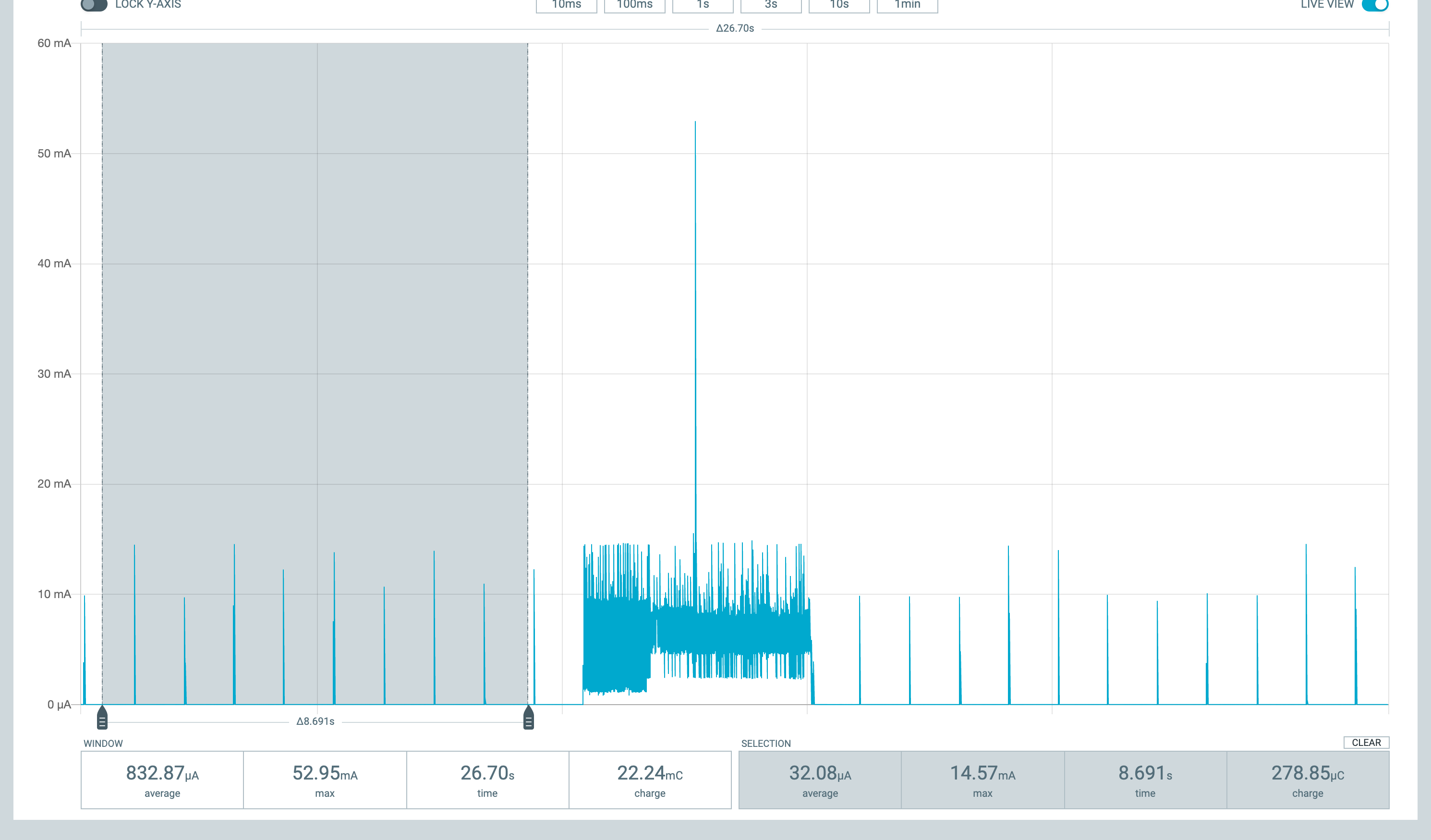 Figure 3. Current consumption of the BLE node
The figure above shows a full sleep-wakeup-display-sleep cycle. In the highlighted are, the system is in deep sleep, while only the radio transmits advertising packets with a period of one second. The current consumption averages at 32 uA, which is good. I believe there’s still room for shaving off some extra microamps, though, by being more fine-grained about which systems/GPIOs to turn off. This online power profiler from Nordic sets a good baseline for what’s possible, and we can go as low as ~10 uA while advertising.
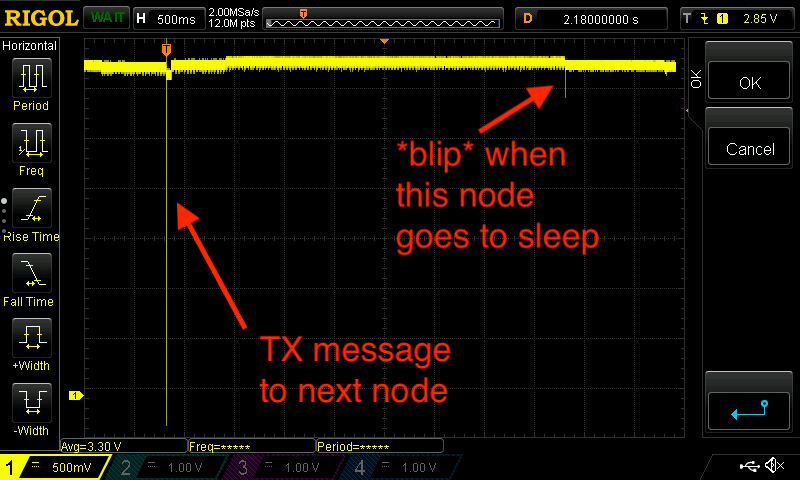 Figure 4. An oscilloscope plot of the
 RX-TX line between the BLE node and the first UART node
There is a small extra complication in this setup. In the figure above, there is a delay between the BLE node forwarding a “sleep” message to the next node and the BLE node itself sleeping. This is due to the time it takes the client to disconnect from the BLE node after writing a message, and it’s somewhat exaggerated here. When it does go to sleep, there’s a little blip in the RX-TX lines between these nodes, and its enough to wake the next node up right after it went to sleep.
I think the blip is likely due to the TX GPIO of the sleeping node transitioning into a high impedance mode. I tried not shutting down this specific GPIO before sleeping, but that did not help.
I experimented with a couple of solutions: a pull-up resistor, an RC filter. In the end, the best solution was the simplest - just synchronizing this dance:
To handle a "sleep" message:
  - **Wait for a little while so the previous node can blip into deep sleep**
  - Forward the sleep message to the next node
  - Go to deep sleep
UART Nodes
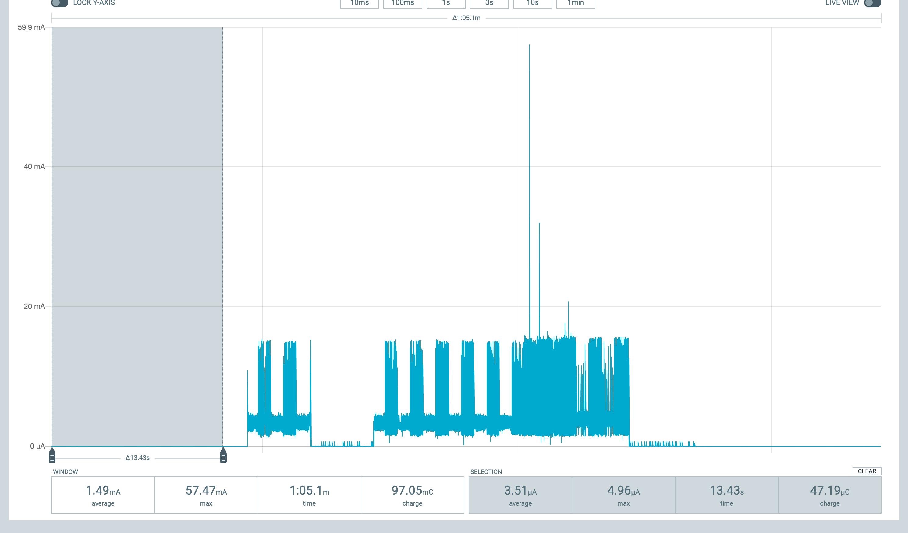 Figure 5. Current consumption of a single UART node
With our topology choice, all UART nodes have the luxury of having their radio off. In addition to some experimentation on which GPIOs to shutoff pre-sleep, they average at around 3.5 uA when in deep sleep.
At this point I also lost a few hours trying to figure out why shutting down all GPIOs yielded a much higher current consumption, in the order of 10 mA. It turns out at least one of the GPIOs controls the power to the e-ink display, and if you call shutdown_gpio on this specific pin, the display will be turned on all the time. So not that one.
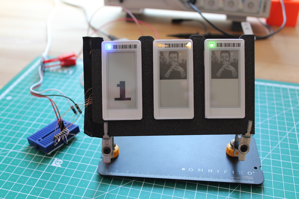 Figure 6. Front shot of the second prototype. Three ESLs linked together. We can also draw dithered black & white images
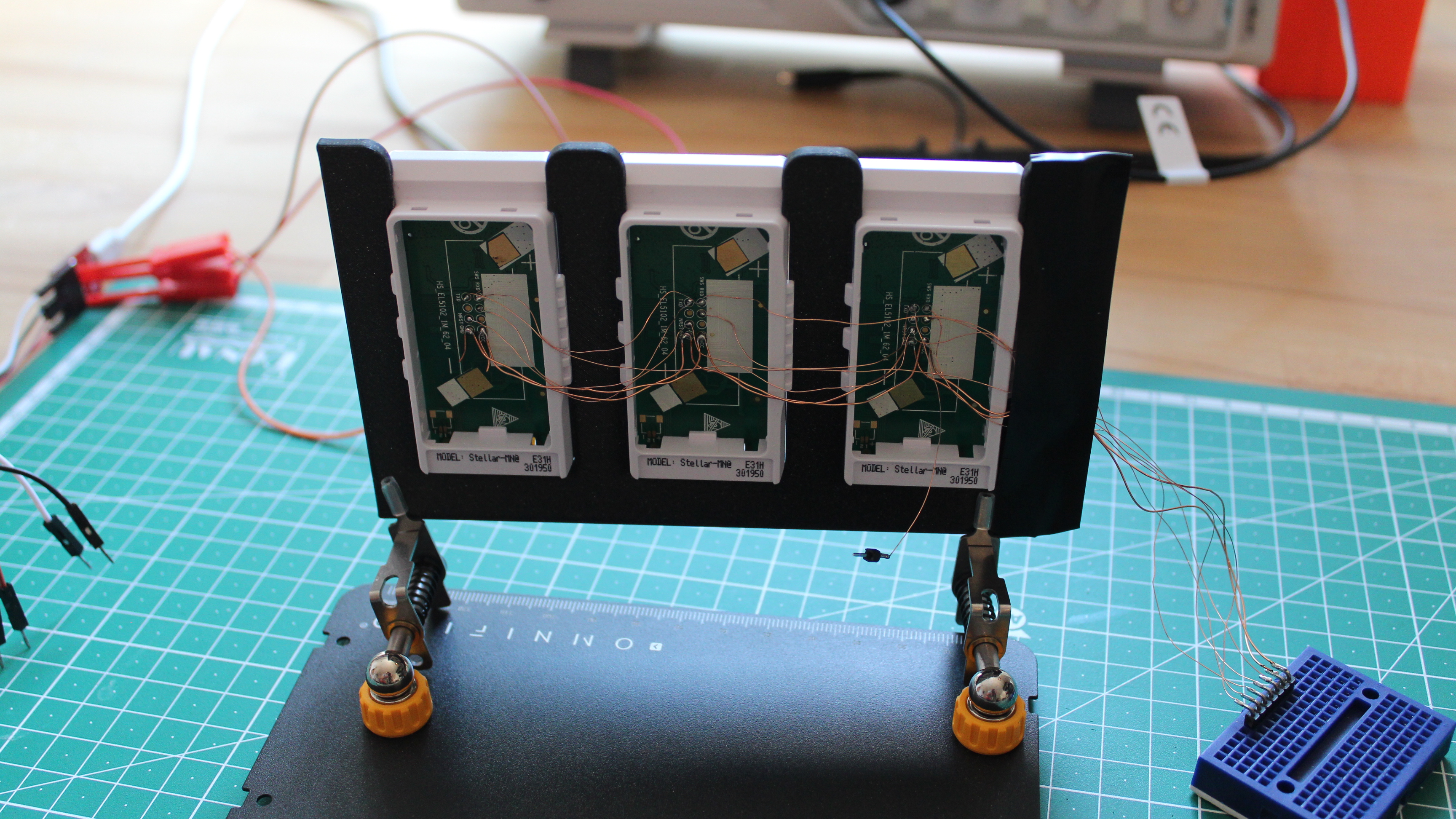 Figure 7. Back shot of the second prototype. Three ESLs linked together
Go Big or Go Home
The end goal was to use up almost all the 25 ESLs I had. I had broken one and given one to a friend. To have some room for error, I settled on a 2x10 panel.
I measured the ideal wire length between a TX-RX pair and designed this little odd-shaped spool to try and make the wiring tidier:
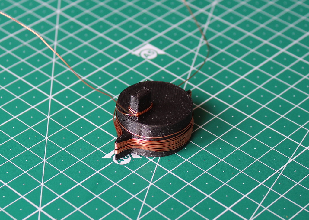 Figure 8. Winding wire around this spool makes all segments equally spaced. Skipping the notch yields the correct length between two horizontal rows
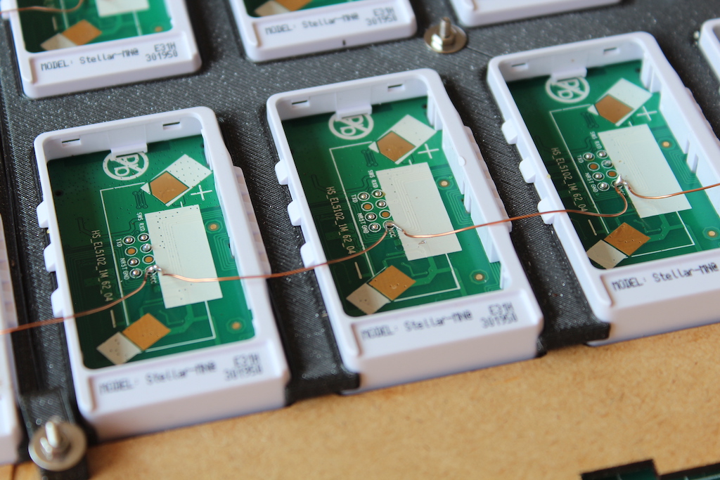 Figure 9. The unwound wire has these convenient indentations that dip into the back of the cases to reach the test pads
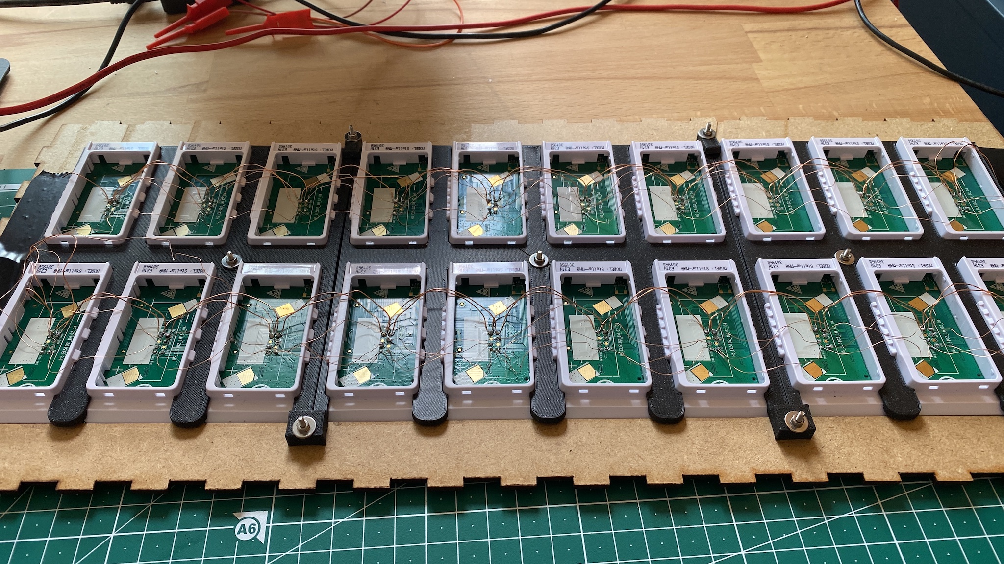 Figure 10. 4 meters of wire and 120 solder points. Not as pretty as I hoped for
At this point I wasted half of my brain power on being extra mindful not to accidentally get the wires hooked on something while moving around. I am confident that would rip the test pads right out and destroy the PCB traces of multiple ESLs at once.
Fast Flashing
The design decision of having the same firmware for all UART nodes paid off even better than expected. As it turns out, I can wire up all the programming ports on the nodes and flash all of them at once, too. I was just hoping to avoid 20 compilations, but I’m happy to have found out I can also avoid flashing the same firmware 20 times, which is even slower.
Clients
To talk to the array and command it to draw stuff, I initially put together a hacky Python CLI. It talks to the assembly either via BLE or UART, and you can use it to draw stuff like this:
# Example 1. Draw the letters H e l l o starting from node 0.
$ python main.py --transport=ble char --invert --font press_start_50 "Hello"
# Example 2. Draw the string "ok" on the 3rd node at coordinates y = 30, x = 10.
$ python main.py --transport=uart --to=2 str 30 10 "ok"
# Example 3. Send all nodes into deep sleep.
$ python main.py --transport=ble sleep
# Example 4. Flip an LED on the 8th node.
$ python main.py --transport=ble --to=7 ping
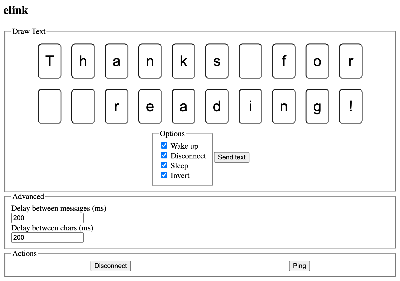 Figure 11. A Spartan web client for elink. To see the result of pressing the “Send text” button, scroll to the end of this post
To make it easier for friends and family to use it, I also put together a quick and dirty web client (source). It uses the Bluetooth Web API to connect to elink via BLE.
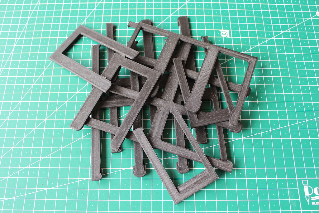
The Case
I wanted the finished project to both feel sturdy and look nice on my wall. The first part I designed was a snap-fit frame for an array of ESLs. It took more than a few iterations, but it turned out okay:
Figure 12. Snap-fit support for six ESLs. Sound on for maximal satisfaction
For the enclosure, I just really wanted an excuse to learn how to use a laser cutter. I experimented with different materials, laser settings and learned about kerf in the process. I used boxes.py to generate an SVG with the case blueprints and tweaked the results in Inkscape. The final plans are here.
I settled on a 3 mm laser-cutting-safe composite wood sheet I found in the scrap bin.
Figure 13. Laser-cutting the front panel
Figure 14. Engraving the back panel
Figure 15. Assembling the case. The most satisfying part of the project
Result
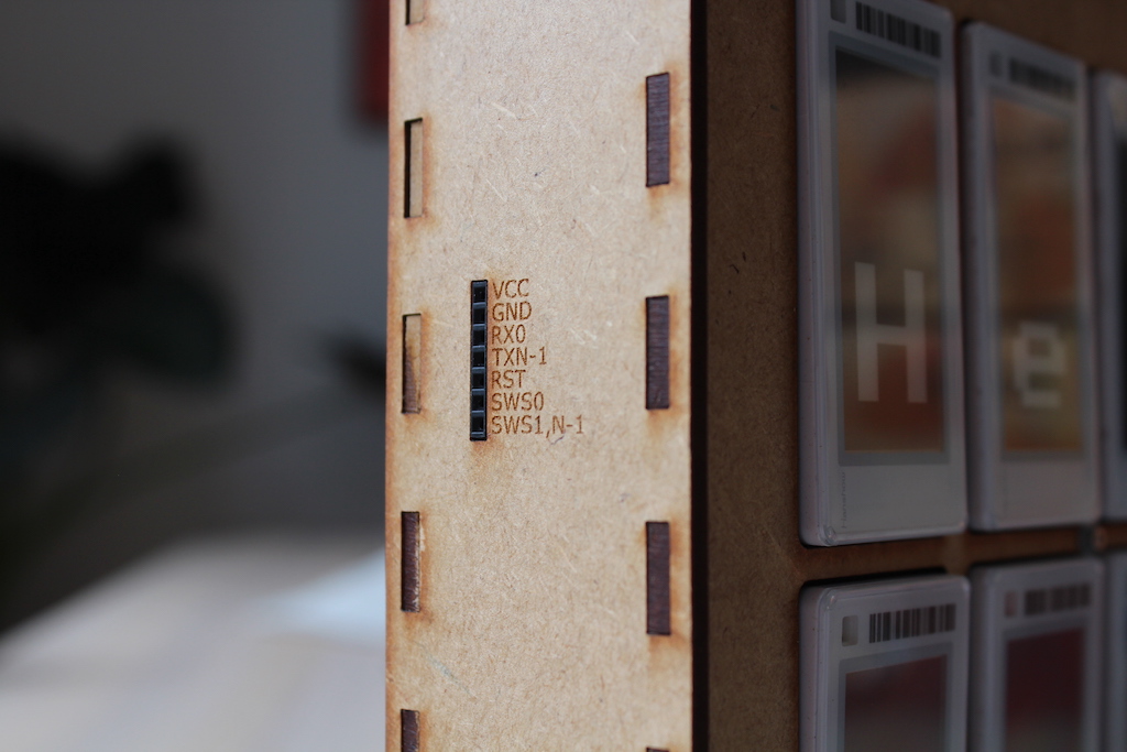 Figure 16. Programming ports with engraved labels
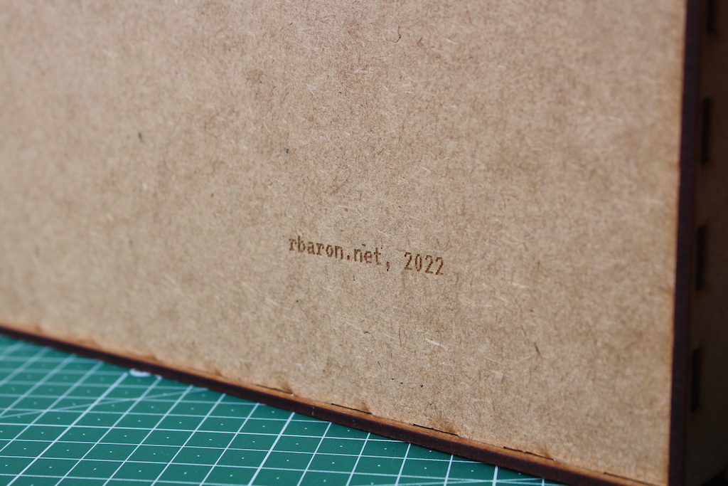 Figure 17. Engraving on the back
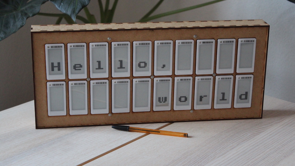
Figure 18. Drawing “Hello, world”
Parting Thoughts
I’m pleased with the journey and the result. The ESLs are a little bit more reflective than I anticipated, due to its plastic enclosure and not the display itself. I am looking forward to seeing how well they hold up against the ambient UV light in one year time, as I had one e-ink display degrade to an unreadable point.
For power, I planned on running the whole array off a LiPo cell, and estimated the battery life of over a year. I assembled a charger circuit with a 3.3V regulator. After realizing how hot it gets while charging, I decided against enclosing it in a wooden case. I am running the system directly off a pair of off-the-shelf AA batteries. At ~100 uA deep sleep, they should last for a while.
The full code for the firmware and the clients, as well as files to build the case, are available on github.com/rbaron/elink.
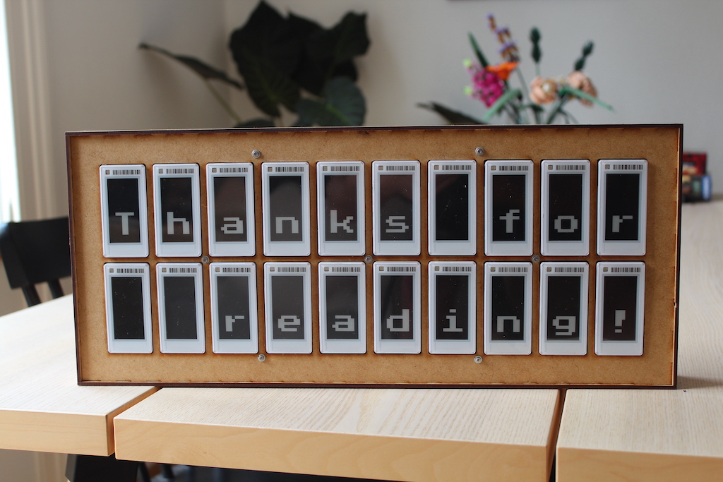 Figure 19. Thanks for reading
If you enjoy posts like this, consider following me on twitter.