Following a year and a half of sitting inside the house, I set out to improve my wellbeing by getting a new fitness tracker. It worked out better than I expected - hacking on it kept me busy for a couple of months - at the small price of making me sitting inside the house even harder.
Before starting, I stated my goals as follows. I wanted to:
- Understand its hardware
- Figure out how to talk to it
- Dump its stock firmware
- Get it to run custom code, ideally making use of its:
- GPIO pins (both for input and output)
- Color display
- Bluetooth low energy (BLE) capabilities
I documented the process of going through these goals in the following sections. It’s been an incredibly fun journey. I hope you enjoy it as much as I did.
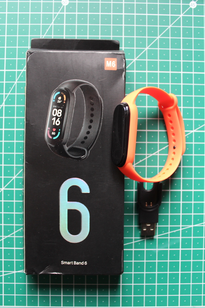
The M6 Fitness Tracker Bracelet(s)
The particular bracelet we are talking about is the M6 from AliExpress (screenshot). I believe the name is an attempt to piggyback on the popularity of the $50, entry level Xiaomi Mi Smart Band 6 fitness tracker. At a $6 price point, our device is an even entrier level bracelet, and to put it politely, it draws a lot of inspiration from the Xiaomi one.
Hardware Overview
Disassembling the plastic case is so easy that it’s difficult to trust the IP67 water resistance rating claimed on the box.
Inside, we see some interesting stuff:
- A Telink TLSR8232 system-on-a-chip (SoC)
- A 0.96” (160x80 px) color display
- A tiny ~100 mAh LiPo battery and USB charging circuit
- A vibration motor
- A (most likely) fake heart rate sensor
The Brains
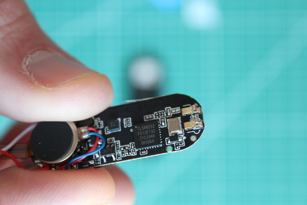
The SoC in the M6 is a Telink TLSR8232 (datasheet). Some specs:
- 32-bit CPU
- Closed architecture (usually referred to as tc32, similar to ARM9) - not a lot of resources about it
- 24 MHz clock speed
- 16kB of SRAM
- 512kB of internal flash
- 32kHz onboard oscillator for low power mode
- SWS (Single Wire Slave) interface for debugging and programming
- Integrated Bluetooth Low Energy (BLE) transceiver
- Low power operation (alleged ~2 uA in deep sleep)
As luck would have it, just a few months ago I had seen a Telink chip in my little, hackable Xiaomi thermometer. At the point, I re-flashed it with @atc1441’s alternative firmware. Even though it’s a different SoC model, this gave me a little hope and a valuable starting point.
Exposed Pads
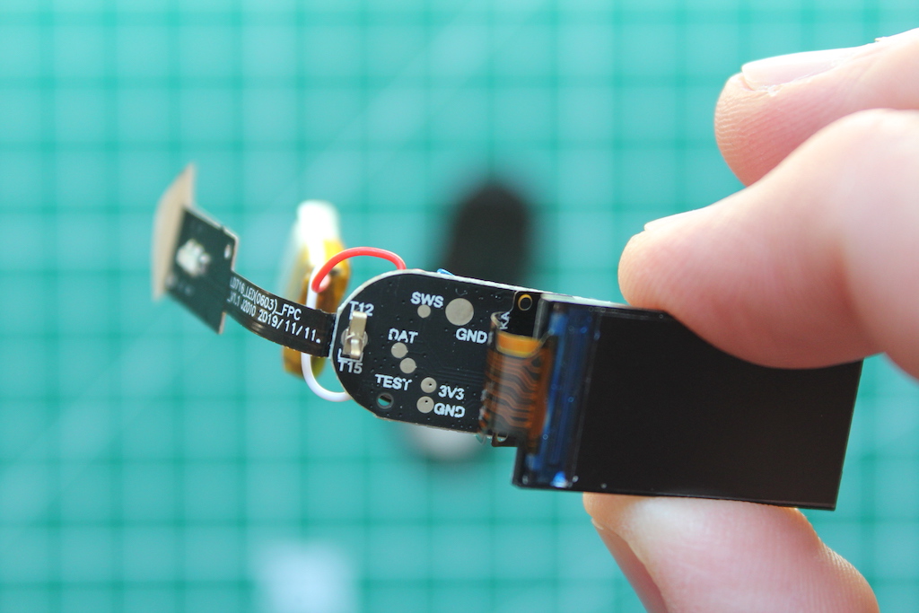
Armed with nothing but a multimeter, a datasheet and good intentions, I tried to find where these pads are connected to. This is what I came up with:
| Pad | SoC Pin # | SoC Pin Label |
|---|---|---|
| SWS | 01 | SWS/ANA_C<7> |
| DAT | 06 | ANA_A<4> |
| TEST | 27 | ANA_C<1> |
| TX | 18 | ANA_B<4> |
| RX | 19 | ANA_B<5> |
The Single Wire (aka. SWire or SWS) Interface
Now that we identified the brains of the bracelet, we turn to the goal of actually talking to it. If you programmed an ESP32 before, you probably relied on its bootloader and talked to it via UART. If you programmed or debugged an ARM microcontroller before, you probably used the SWD (serial wire debug) protocol.
In Telink-land, the analogous interface is called Single Wire or SWire. This is how apps are loaded into its flash memory, how it’s memory is read and written and how it’s debugged at runtime.
The real fun begins, though, when we try to learn more about this interface. The datasheet is almost comically quiet about it, as if pretending it doesn’t exist.
In the real world, where real programmers do real work, these chips are flashed and debugged with Telink’s official Burning and Debugging Tool. In the past, it seems hobbyists could get these devices very easily, but I couldn’t find them on the usual places in the beginning of the project. Now, as I write this post, it seems they recently became available on Mouser.
While the lack of specs and programmer set the stage up for a very unsatisfying dead end, this is, in fact, where things start to get interesting. The deep dive into the SWire specs and alternative tooling has been the most rewarding part of the project. Read on.
The Missing Specs
In what could be the nerdiest Indiana Jones spin-off yet, “the search for the missing SWire specs” brought me to the work of pvvx. Victor, in addition to maintaining a forked and low-power-optimized version of the alternative Xiaomi thermometer firmware from earlier, is a bona fide SWire ninja.
I struck gold when I came across one of his repositories, the TlsrTools. In there, there’s an excerpt of a PDF that contains a brief, two-page description of the SWire protocol. This seems to be a part of an old version of a Telink datasheet that has since been chopped off. That’s great news. We’re back in the game.
The Alternative Programmer
Victor also bootstrapped a whole new open source programmer for some Telink chips based on the beloved and ubiquitous STM32 Blue Pill board. This means that potentially both our roadblocks are removed - we have a (terse) SWire interface spec and a programmer.
At this point I start to really enjoy the process of demystifying SWire. It reminded me of the heartwarming story of when Paul McCartney and John Lennon got on a bus across Liverpool to meet a fellow they heard knew about the B7 chord. Now here I am, getting on the proverbial bus to meet this single fellow I heard knew about the SWire interface.
The bus takes me to interesting places. I can’t recognize the street signs, but the view looks amazing. I imported the STM32 code into my editor and translated some of its Russian comments.
This cross-language detective work gave me a relatively good understanding of the SWire protocol and of how to use Victor’s alternative programmer. There’s still a remaining pressing question, though. Victor’s programmer is made for TSLR826x chips, and we’ve got a TLSR8232 chip on our hands.
From Pascal to Python
There are usually three moving parts when programming/debugging a chip:
- The target board we want to program
- The programmer hardware
- The computer software that talks to the programmer
In Victor’s alternative programmer, the computer software is a Pascal, Windows-only application. I think it is a prime example of getting real stuff done with the language at hand.
The role of the computer software is to send commands to the programmer hardware and get it to read/write data from/to the target board. As I don’t have a Windows box at home, I implemented a barebones Python script, the tlsr82-debugger-client.py that works as the computer software component.
We can now use this Python script and the STM32 to hopefully speak SWire with our M6 bracelet. The setup is as follows:
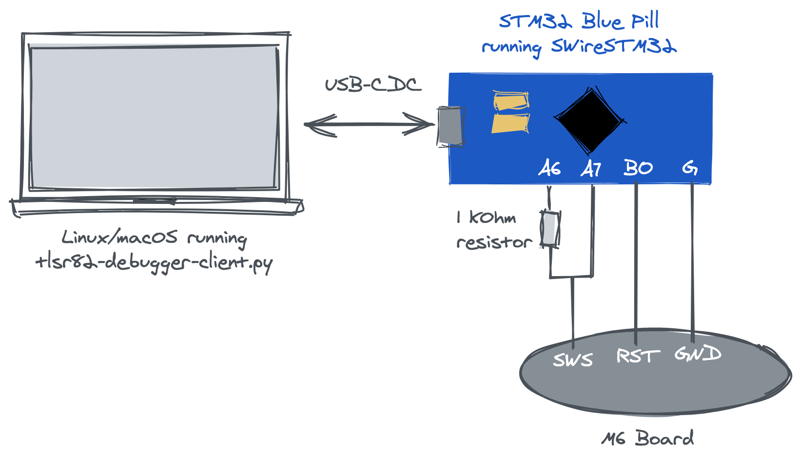
SWire Protocol Overview
Let’s take a dip into the mysterious SWire spec.
As the name suggests, a single wire is used for transmitting data back and forth between two devices. In our case, the STM32 programmer (the master) and the target board (the slave). There is no separate clock line as in SPI or I2C. The single wire topology allows for both devices to speak, but they cannot speak at the same time. In other words, we can call SWire an asynchronous, half-duplex interface.
These two key aspects of SWire imply that:
- Asynchronous: since there’s no shared clock, both devices must somehow employ compatible reading & writing speeds
- Half duplex: each device must know when it should listen to messages and when it’s allowed to transmit messages. There must be a precisely choreographed dance between the two parties
To achieve coordination, the SWire protocol attributes responsibilities to the master and slave devices. The master is responsible for initiating the communication and managing the bus logic level between data transfers. The slave is responsible for sending data when it’s expected to. I put together some real-world examples below to make this clearer.
Sending a Single Bit
The first thing to notice is how bits are encoded in the wire. Each bit is transmitted in five units of time:
- To send a
0, keep the voltage low for one unit and high for4units; - To send a
1, keep the voltage low for4units of time and high for1unit;
To make matters concrete, here is a real SWire transmission I captured with a logic analyzer:
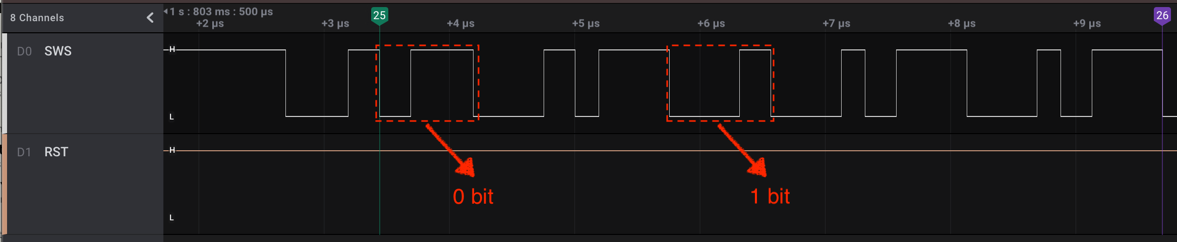
In the above screenshot, there are 8 bits being transmitted between the flags marked as 25 and 26. Can you decode these 8 bits? If you’re feeling brave, let me know your answer.
Sending a Single Byte
We now know how individual bits look in the wire. To transmit a full byte, the SWire protocol specifies that 9 bits are needed:
- Bit 1: The cmd bit.
0specifies that the message contains data and1specifies that the message is a command - Bits 2-8: The message content (8 bits)
- One time unit of low level to signal the end of the message
Again, let’s take a look at a real-world example transmission of a 0xb0 byte:
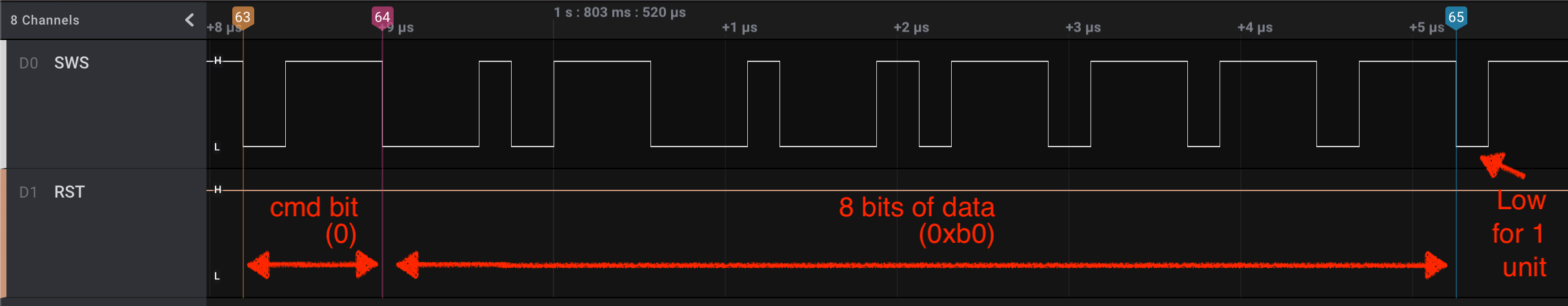
After the last unit of low is sent, the bus is released and goes back to it’s natural high voltage. In other words, the SWire data bus is pulled high.
Write Requests
We saw how individual bits and bytes are encoded in the wire. Next, let’s take a look at how the SWire protocol specifies a byte to be written at a specific address. In this scenario, the master wants to write a byte b to the address addr in the slave’s memory.
To do so, the master must send a sequence of bytes, each one encoded as described in the section above:
- The
STARTbyte. This one always has the value0x5a - The most significant 8 bits of the target
addr - The least significant 8 bits of the target
addr - The
RW_IDbyte. The most significant bit should be set0for writing operations - The byte value
b - The
ENDbyte. It always has the value0xff
Let’s look at the following example:
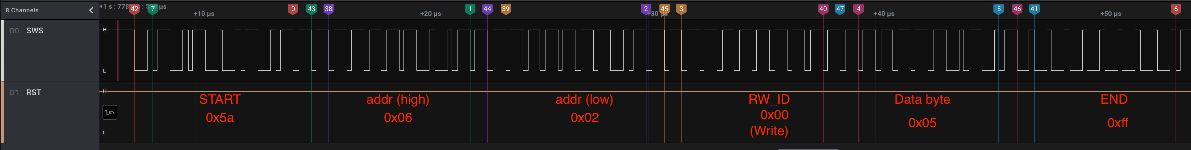
In this example, we can see the byte 0x05 being written into the slave’s memory address 0x0602.
Variations of the SWire Protocol
It’s worth noting that there exists at least one variation of the SWire protocol. In the other variant, the master sends 3 bytes of addr after the START byte, instead of only two bytes in our SWire protocol. The 3-byte variant is employed, for example, in Telink’s TLSR8251 SoCs, used in the Xiaomi thermometer we mentioned above. In the Python-based flasher in ATC_MiThermometer repository, we can see where the 3 bytes of addr are specified in the read/write requests from the master to the slave device.
Writing multiple bytes
That’s a lot of overhead for writing a single byte. Luckily, the protocol let’s us write multiple data bytes at once. To do so, the master simply sends a sequence of bytes instead of a single byte like in the example above.
Read Requests
Read requests are very similar to write requests. There are only two important differences:
- The most significant bit of the
RW_IDbyte is set to1 - Instead of sending data after the
RW_IDbyte, the master reads data from the SWire data line
Again, take the following example. To make things more interesting, in this example the master reads two bytes from the slave:
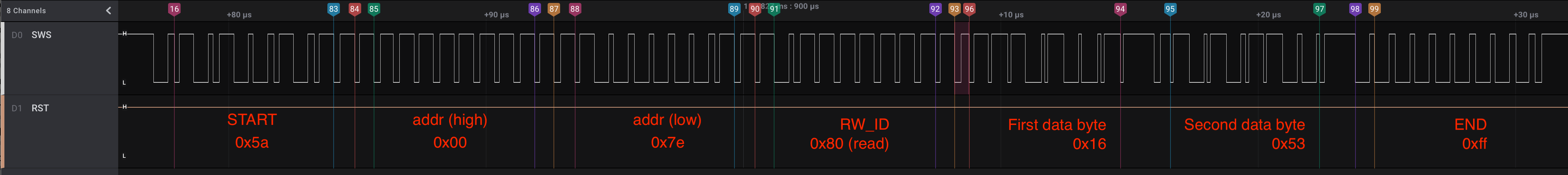
After sending the RW_ID byte, the master sends one unit of low level. The slave responds with 8 bits of data and one unit of low level. The master can request more data by writing a single unit of low level, otherwise the master sends the END byte (0xff) and the transmission is over.
Let’s zoom into the transmission of multiple bytes during the read request, just after the RW_ID byte above:
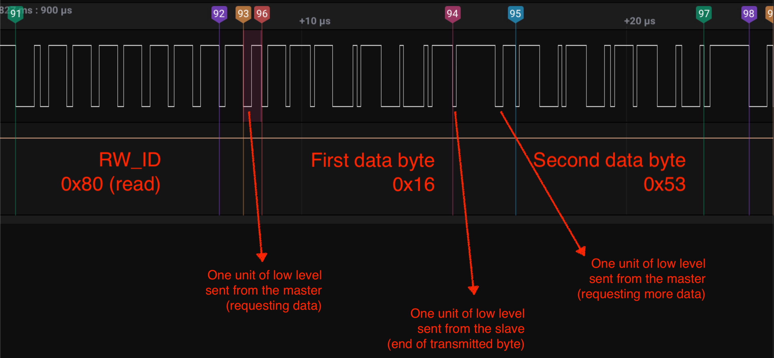
In this example, the master reads the value 0x5316 from the slave’s address 0x007e.
The address 0x007e we just read is, in fact, a special register in the TLSR82xx chips. It holds the “Chip ID”. For our TLSR8232, the Chip ID is 0x5316.
You can find this whole annotated logic analyzer capture in get_soc_id.sal. It includes reads and writes requests.
Speed Mismatch Hazard
The above read example, we saw that both the master and slave read and write to the same bus. They must understand each other’s messages. A crucial setting is the speed at which both devices transmit data.
Let’s turn to the following pathological example. It is the same read request for address 0x007e as above:

Take a look at what happens after the master sends it’s RW_ID byte. The slave starts responding, but with at a visibly lower speed. We can see that the bits are encoded in much wider windows than the previous ones sent from the master. Also note that, even though the whole transmission failed, the beginning of the slave’s response seems promising. It’s starts with 0x16, which is the expected first byte of the “Chip ID”.
This speed mismatch is a problem. It breaks the precise dance that the master has to coordinate. But not all is lost - from this observation we can draw two important conclusions - a bad one and a good one
- Bad one: To read data, the slave’s speed has to be compatible with the master’s speed, otherwise the master fails to coordinate the whole operation. I believe we could find a solution that adjusts this speed and gets the master to adapt its pace to the slave’s speed, but this is not currently done
- Good one: Writing data seems to be a less coordination-sensitive operation. As we noted above, the slave seems to have been able to correctly understand the bytes sent from the master (which spell “read request for address
0x007e”), even though the slave itself is misconfigured with a slower speed
The last piece of the speed puzzle is that we can configure the slave’s speed by writing to one of its special registers. From the “missing SWire spec”, we see a little note about the register at the address 0xb2:
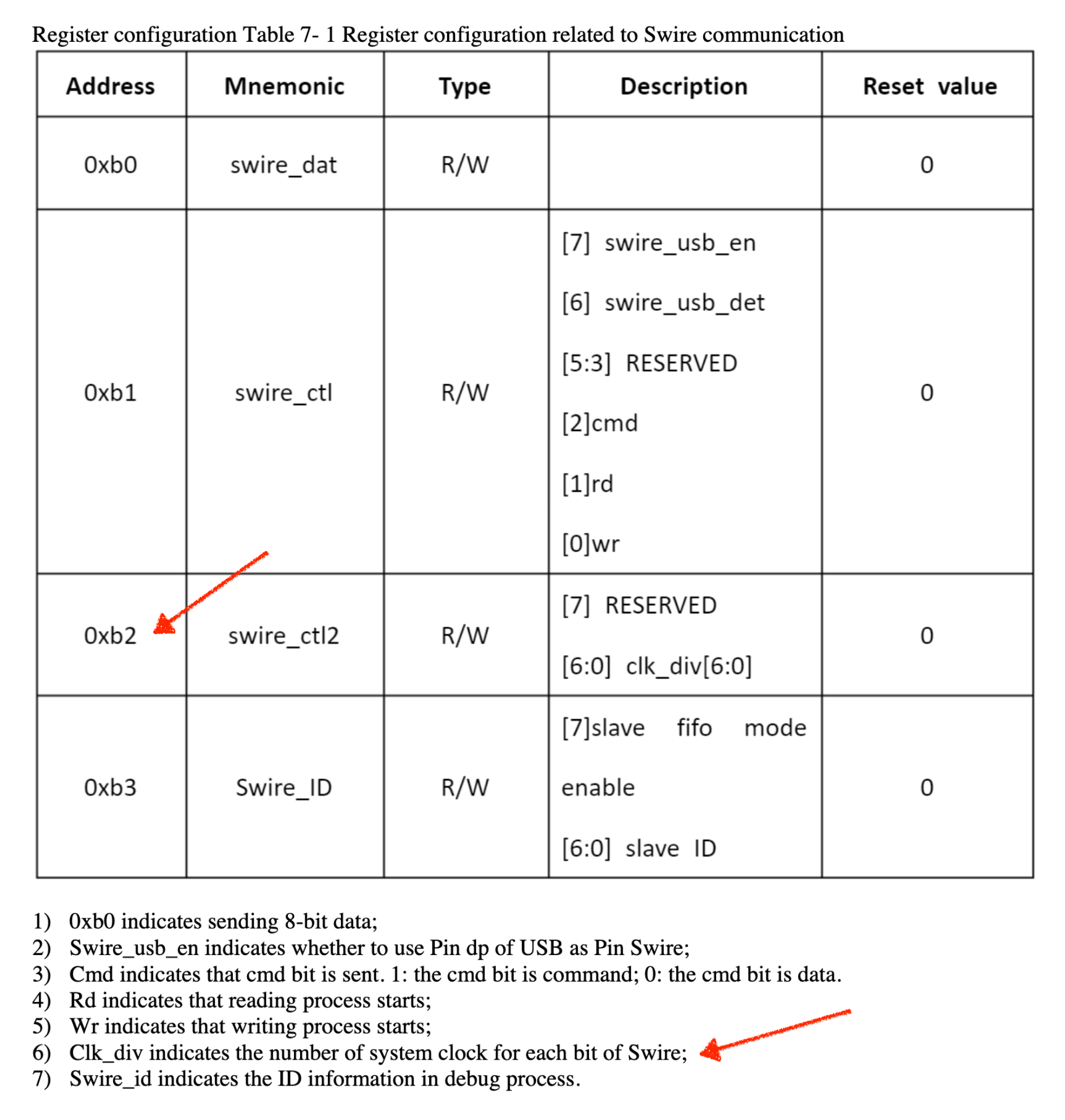
In short, we can tune the slave’s SWire speed by writing to it’s 0xb2 memory address.
On the other end, we also need to set up the master’s SWire speed.
The strategy that has worked is to fix the master’s SWire speed at a reasonable value and try a few possible speeds for the slave. This is precisely what our Python script does (edited for brevity):
# Writes the value `speed` into the slave's 0x00b2 register.
def set_speed(speed):
    return write_and_read_data(make_write_request(0x00b2, [speed]))

def find_suitable_sws_speed():
    for speed in range(2, 0x7f):
        set_speed(speed)
        try:
            get_soc_id()
        except Exception:
            continue
        else:
            print(f'Found and set suitable SWS speed: {speed}')
            return speed
    raise RuntimeError("Unable to find a suitable SPI speed")

def init_soc(sws_speed=None):
    ...
    # Set up the master speed.
    set_pgm_speed(0x03)

    # If the user specifed a slave speed, use that.
    if sws_speed is not None:
        set_speed(sws_speed)
    # Otherwise try many different ones until one works.
    else:
        find_suitable_sws_speed()
Invalid CPU State Hazard
Another tricky trap is the fact that sometimes the slave’s CPU does not seem to respond to SWire requests. I haven’t found the precise reason, but my guess is that SWire doesn’t work when the slave is in some power saving mode or has interrupts disabled.
In practice, it means that it can be difficult to start a SWire exchange depending of the program that is running on the target device. To overcome this, pvvx’s strategy is to:
- Reset the device (by pulling it’s RST pin low)
- Start bombarding the target device with “CPU stop” SWire commands while the RST pin is pulled high
The objective here is to reach the CPU in a good state as it resets, before the application messes up with it too much.
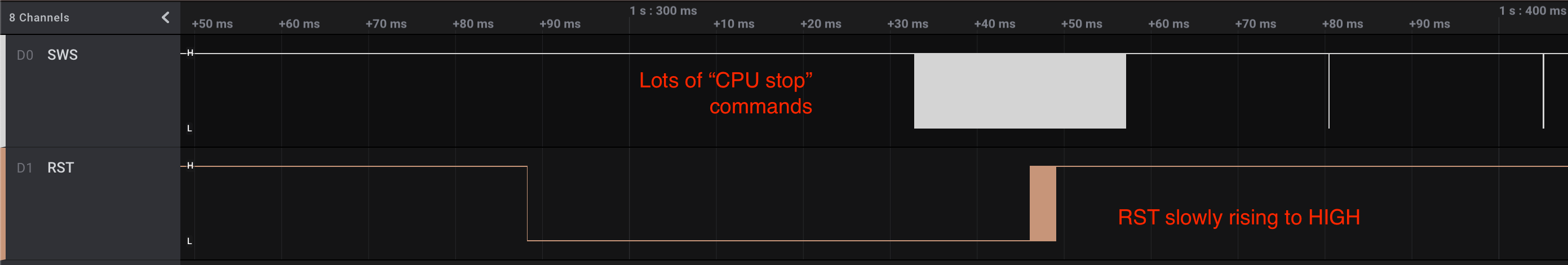
For the extra curious reader, the “CPU stop SWire command” is a simple write request of 0x05 to address 0x0602. This address corresponds to a special register that controls the CPU state.
Getting to the RST Pin
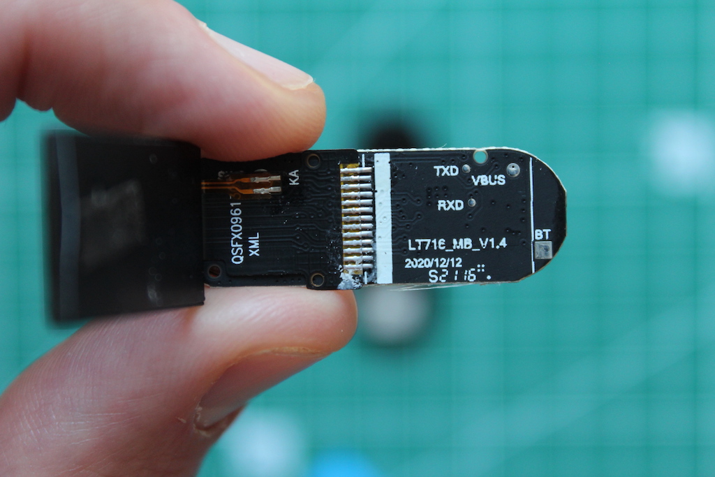
The RST trick above works really well. The only downside is that, if you look at the M6 board, the RST pin is not broken out in any pad.
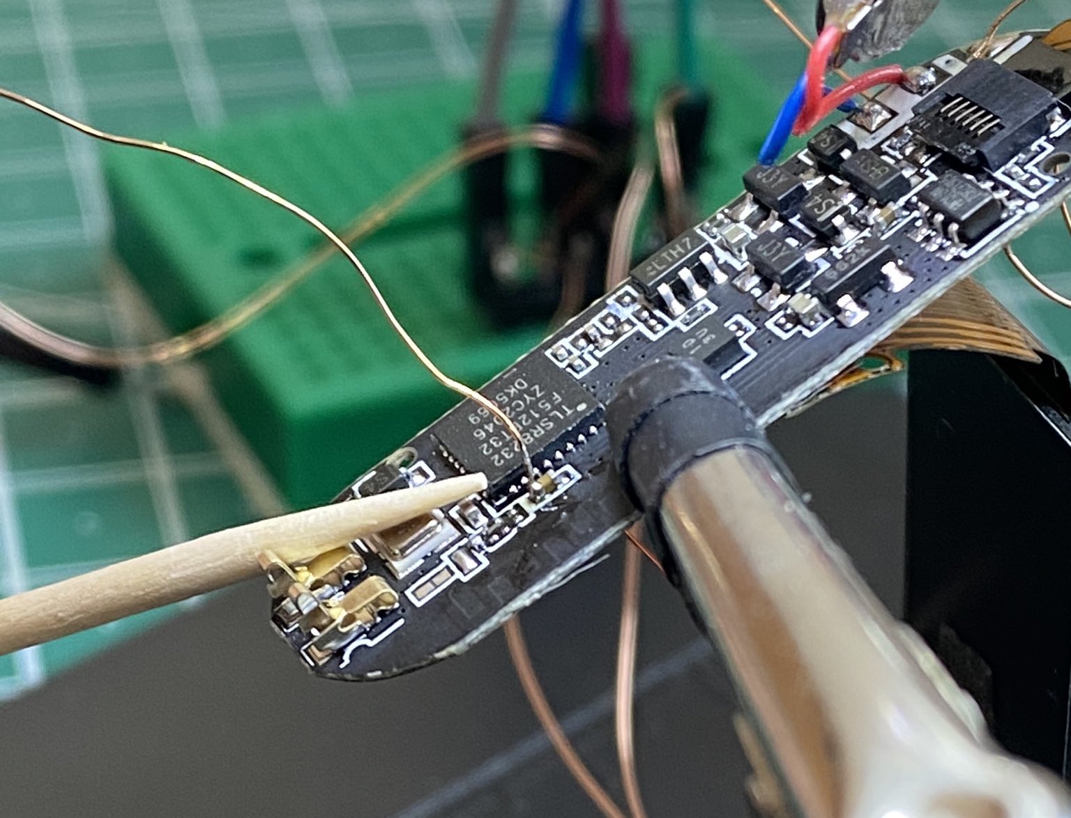
In the datasheet, we can see that the TLSR8232 RST is on pin 26. On the M6 board, this pin connects directly to a tiny capacitor, as shown in the photo above. This is a tricky soldering job, but it’s doable with a pre-tinned wire and a little bit of flux.
Alternative Tricks - No RST Soldering Required (Possibly)
While having the RST pin available makes life easier and working with SWire more predictable, it might not be strictly necessary. Two ideas to get around it:
- Just try it without the RST pin. You might find that it just works. In fact, if you look at how the Xiaomi thermometer alternative firmware is flashed, you will find out that the RST is not needed there
- As a last resort, you can try to manually power cycle the target board while the “CPU stop” bombardment is going on. You might try to tweak the code to increase this time window
Reading the SoC ID
With the content we covered so far, we are ready to take a look at a real-world scenario. Using the tlsr82-debugger-client.py Python script to read the target device’s memory:
% python tlsr82-debugger-client.py --serial-port /dev/cu.usbmodem6D8E448E55511 get_soc_id
Trying speed 2
Trying speed 3
Trying speed 4
Trying speed 5
Trying speed 6
Trying speed 7
Found and set suitable SWS speed: 7
SOC ID: 0x5316
Behind the scenes, this invocation takes some of the steps we covered previously:
- Reset the target board by pulling RST low
- Bombard the target board by writing many “CPU stop” values to its CPU control register while RST is pulled high
- Set up the master’s SWire speed
- Iterate over possible SWire speeds for the target board until a suitable one is found
- Issue a 2-byte read request to address
0x007e
Reading and Writing to the Internal Flash Memory
One of our goals is to dump the target board’s firmware. It is stored in the board’s internal flash memory. While the details fo the SWire protocol are not public, Telink does offer a SDK for the TLSR8232 SoC. In there, there is an interesting file in ble_sdk_hawk/drivers/5316/flash.c that contains the code for the chip to read and write to its own internal flash - comments are my own:
_attribute_ram_code_ void flash_write_page(unsigned long addr, unsigned long len, unsigned char *buf){
  unsigned char r = irq_disable();

  // Writes value 6 to register 0x0d (spi control register).
  flash_send_cmd(FLASH_WRITE_ENABLE_CMD);
  // Writes value 2 to register 0x0d (spi control register).
  flash_send_cmd(FLASH_WRITE_CMD);
  // Writes 3 bytes of the target address to register 0x0c (spi data register).
  flash_send_addr(addr);

  unsigned int i;
  for(i = 0; i < len; ++i){
    // Write data byte to register 0x0c (spi data register).
    mspi_write(buf[i]);
    mspi_wait();
  }
  // Chip select high.
  mspi_high();
  flash_wait_done();

  irq_restore(r);
}

_attribute_ram_code_ void flash_read_page(unsigned long addr, unsigned long len, unsigned char *buf){
  unsigned char r = irq_disable();

  // Writes value 3 to register 0x0d (spi control register).
  flash_send_cmd(FLASH_READ_CMD);
  // Writes 3 bytes of the target address to register 0x0c (spi data register).
  flash_send_addr(addr);

  // Dummy write to register 0x0c (spi data register).
  mspi_write(0x00);
  mspi_wait();
  // Writes value 0x0a to register 0x0d (spi control register).
  mspi_ctrl_write(0x0a);
  mspi_wait();
  /* get data */
  for(int i = 0; i < len; ++i){
    // Reads byte from register 0x0c (spi data register).
    *buf++ = mspi_get();
    mspi_wait();
  }
  // Chip select high.
  mspi_high();

  irq_restore(r);
}
We can see that interacting with the internal flash boils down to writing to the target board’s SPI control register (at address 0x0d) and reading/writing to the SPI data register (0x0c), as well as manipulating the SPI chip select logic level.
Since we know how to interact with the target board’s memory addresses via SWire, we can implement the exact same operations in our Python script, targetting reads and writes to the SPI control and data registers (0x0d and 0x0c, respectively). This is exactly what I did. For instance, check out the write_flash function:
def write_flash(addr, data):
    send_flash_write_enable()

    # Chip select low.
    write_and_read_data(make_write_request(0x0d, [0x00]))

    # Write command.
    write_and_read_data(make_write_request(0x0c, [0x02]))

    # Flash address.
    write_and_read_data(make_write_request(0x0c, [(addr >> 16) & 0xff]))
    write_and_read_data(make_write_request(0x0c, [(addr >> 8) & 0xff]))
    write_and_read_data(make_write_request(0x0c, [addr & 0xff]))

    # Write data
    write_and_read_data(make_write_request(0x0c, data))

    # CNS high.
    write_and_read_data(make_write_request(0x0d, [0x01]))
The read_flash function works similarly.
Dumping the Firmware
With the ability to read the target board’s internal flash over SWire, we can now dump the M6’s firmware:
$ python tlsr82-debugger-client.py --serial-port /dev/cu.usbmodem6D8E448E55511 dump_flash flash.bin
Found and set suitable SWS speed: 7
Dumping flash to flash.bin...
CPU stop.
CSN high.
0x000000 00.00%
0x000100 00.05%
0x000200 00.10
...
0x07cd00 99.85%
0x07ce00 99.90%
0x07cf00 99.95%
Writing 512000 bytes to flash.bin
You can find the raw dump in the project’s repository, under dumped/flash.bin.
SDK, Compiler & Docker Image
With the first major goal of dumping the firmware behind us, we now turn to the challenge of running our own code on it. The first step is to get the SDK and compiler for the TLSR8232.
The SDK is available on Telink’s website. The one I used is listed in the “Bluetooth LE Generic” section. Unpacking the SDK reveals it’s integrated with Telink’s own IDE, which is based on the Eclipse IDE and seems to be only available for windows. This is fine, but I would love to make things easier creating a single Docker file with all the environment needed for compiling TLSR8232 programs.
Googling around brought me to the Ai-Thinker-Open/Telink_825X_SDK repository. It contains a SDK for Telink chips and it refers to a Linux tc32 toolchain, which is exactly what we need for running it under Docker. I used the tc32 toolchain and the TLSR8232 BLE SDK and set up a Dockerfile that makes compiling our custom code simpler.
With this, we can simply spin up a Docker container and type make to compile our code. We can build the blinky binary by doing:
# In the example-programs directory.
# Build the Docker image from the Dockerfile.
$ docker build -t tlsr8232 .

# Run the Docker containers and mount the current directory into /app.
$ docker run -it --rm -v "${PWD}":/app tlsr8232

# Inside the docker container, compile the blinky example.
$ cd blinky/
$ make
...

# The compiled binary file is in _build/blinky.bin.
$ ls _build/blinky.bin
_build/blinky.bin
Blinky
The time has come. We now have all the tools and knowledge to compile and burn our own little firmware on the M6 bracelet. I hooked up a red LED to the TX pad and set out to make it blink.
The sample code for the blinky can be found in the GitHub repo under example-programs/blinky. Here is the entirety of its main() function:
int main() {
  cpu_wakeup_init();
  clock_init(SYS_CLK_16M_Crystal);
  gpio_init();

  // TX pad.
  gpio_set_func(GPIO_PB4, AS_GPIO);
  gpio_set_output_en(GPIO_PB4, 1);
  gpio_set_input_en(GPIO_PB4, 0);
  gpio_write(GPIO_PB4, 1);

  while (1) {
    gpio_toggle(GPIO_PB4);
    sleep_ms(500);
  }
  return 0;
}
As we did all the hard work of setting up the SDK & toolchain within our Docker image, compiling it is a breeze, as we saw in the previous section. We just have to use our Docker file, mount the example-programs/ repository directory into /app and type make on the example we want to build:
root@c54c8204641d:/app/blinky# make
mkdir -p _build/drivers
...
/opt/tc32/bin/tc32-elf-gcc -c -Wall -std=gnu99 -DMCU_STARTUP_5316 -I /opt/8232_BLE_SDK/ble_sdk_hawk/ -ffunction-sections -fdata-sections -o _build/main.o main.c
/opt/tc32/bin/tc32-elf-ld --gc-sections -T /opt/8232_BLE_SDK/ble_sdk_hawk/boot.link -o _build/blinky _build/main.o _build/drivers/gpio.o _build/drivers/analog.o _build/drivers/clock.o _build/drivers/bsp.o _build/drivers/adc.o _build/asm/cstartup_5316.o /opt/8232_BLE_SDK/ble_sdk_hawk/proj_lib/liblt_5316.a
/opt/tc32/bin/tc32-elf-objcopy -O binary _build/blinky _build/blinky.bin
Burning the compiled firmware in the M6 board is done with our trusty Python script:
$ python tlsr82-debugger-client.py --serial-port /dev/cu.usbmodem6D8E448E55511 write_flash ../example-programs/blinky/_build/blinky.bin
Found and set suitable SWS speed: 7
Erasing flash...
Flash status: 03
Flash status: 00
Writing flash from ../example-programs/blinky/_build/blinky.bin...
0x0000 00.00%
0x0100 03.35%
0x0200 06.71%
...
0x1c00 93.92%
0x1d00 97.27%
Flash status: 00
Immediately after the command finishes, the M6 board should do its thing:
The Capacitive Button
The touch pad in the M6 is not connected directly to the TLSR SoC, but instead passes through a driver IC on the board. I suspect the IC is responsible for managing the touch-sensing circuitry and piping a clean digital signal to the SoC, but I couldn’t easily identify the mysterious IC.
To figure out the corresponding SoC button pin, I used a binary search approach. I first identified all GPIO pins that hadn’t been used yet and set them all up as inputs. I then iterated over them and checked whether or not any of them changed state as I touched the button. If that happened, I toggled the LED. I then partitioned the GPIO pins under test in two groups and repeated the process for that group. It’s not very elegant but I got to the actual pin in no time.
It turns our the button state can be read from the GPIO_PC2 pin. Here’s the result of running example-programs/button firmware:
Display
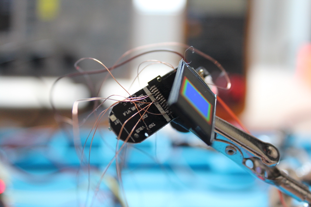
The next goal is to draw something on the display. The first task to identify the hardware. After a lot of googling and guessing, I found the exact same display on AliExpress.
It is a 13-pin, 160x80 px, color SPI TFT display. It’s a little weird that the data lines are called SDA and SCL (which are often seen in I²C devices). I believe they are, in fact, the MOSI and SCLK in disguise.
It uses the ST7735 driver (PDF) to push pixels to the screen. This is good news, as this driver is relatively popular among color displays. It’s featured in many maker-friendly products and supported by Adafruit’s ST7735 library. While Adafruit’s library is built on top of Arduino abstractions and we’re very far from that, it proved to be a great reference.
Next, again, the task is to figure out to which SoC pins the display are connected. Long story short:
| Display pin | SoC Pin # | SoC Pin Label | Function |
|---|---|---|---|
| SDA | 29 | SWS/ANA_C<3> | SPI data |
| SCL | 31 | ANA_C<5> | SPI clock |
| RS | 32 | ANA_C<6> | Data/command selector (D/C# in the ST7732 datasheet) |
| CS | 03 | ANA_A<1> | SPI chip select, active low |
| RST | 02 | ANA_A<0> | Reset pin, active low |
| LEDK | 04 | ANA_A<2> | TFT backlight diode cathode; Driven through a NPN transistor |
To draw a single pixel on the display, we need to take the following actions:
- Turn on the display’s backlight by driving it’s LED cathode (LEDK pin)
- Pull RST high
- Set up SPI with pins SDA & SCL on the target board
- Send a bunch of commands to the ST7735 driver. These include:
- Get out of sleep mode
- Set up the color format (here I’m using RGB565, with 16 bits per pixel)
- Set up the display’s physical dimentions
- Turn the display on
- Send a command to define the drawing region
- Send 16 bits of color for a single pixel
Getting all the details right was not an easy task. Most of the time it feels like working with a black box - there’s no feedback and the error could be anywhere, from the display identification to the pin mapping to the program logic to firmware burning errors.
In the end, through blood, sweat and tears, it finally worked. The example-programs/display draws some color squares in the middle of the screen:
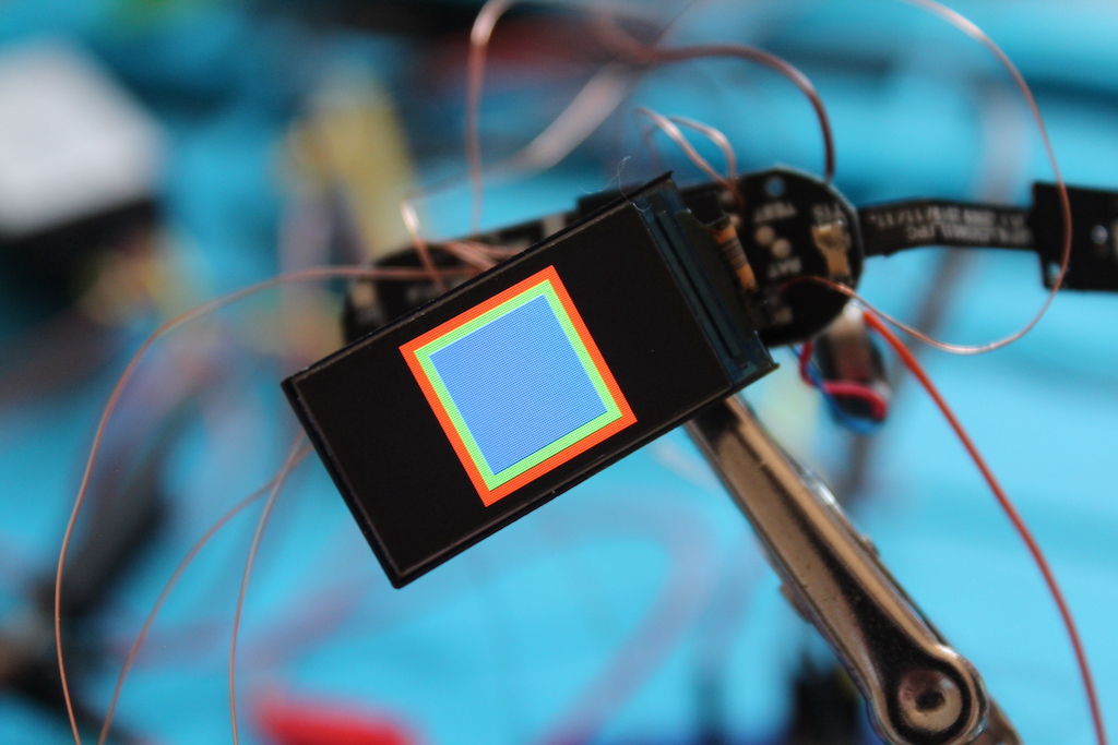
Drawing Text
Given we know how to draw individual pixels on the display, drawing text boils down to figuring out which pixels should be drawn for each character.
A bitmap font fits the bill perfectly. In those, each character is just an array of bits, in which a 0 represents background and 1 represents the pixels we need to draw.
Let’s borrow the Picopixel bitmap font from the Adafruit GFX library.
As an example, if we dig a little bit, we find that the letter A is 3 pixels wide x 5 pixels high and is encoded in the two bytes 0x57 0xda. We start by unrolling those bytes into their binary representation:
0x57 0xda => 0101011111011010
We know this particular character is 3 pixels wide, so we lay that bit sequence into rows, 3 bits at a time:
010
101
111
101
101
And just like magic, if we paint the 1 bits, we see the letter 'A' come up:
 #
# #
###
# #
# #
I implemented this idea in example-programs/text. It’s nice to notice that this algorithm generalizes well for scaling up text. We can target groups of 2x2, 3x3 or 4x4 pixels as if they were one single superpixel.
Bluetooth Low Energy - Peripheral Role
To get started with BLE, I set up the TLSR8232 in peripheral mode and defined a BLE characteristic that toggles an LED when it’s written to. In example-programs/ble-services, I hooked an LED to the TX pad:
In the previous video, I’m using the nRF connect iOS app to connect to the M6 board and interact with the BLE services I defined in the firmware.
Bluetooth Low Energy - Central Role
For the grand finale, I set up to use the M6 as a BLE tracker for another project on mine - the b-parasite soil moisture/air temperature and humidity sensor.
The b-parasite broadcasts its sensor readings via BLE advertisement packets. I thought it would make an interesting demo if I could capture those broadcasts with the M6 and print the sensor values on its display.
As we know the MAC address of b-parasites, we can filter the relevant advertisements with it. Once we identify a b-parasite advertisement, we look into its raw bytes to decode the sensor values:
// BLE advertisement callback. Called whenever a new advertisement
// packet comes in.
int hci_event_handle(u32 h, u8 *param, int n) {
  ...
  event_adv_report_t *p = (event_adv_report_t *)param;
  ...
  // Is this a b-parasite advertisement?
  if (p->mac[5] == 0xf0 && p->mac[4] == 0xca && p->mac[3] == 0xf0 &&
      p->mac[2] == 0xca && p->mac[1] == 0x00 && p->mac[0] == 0x08) {
    ...
    // Decode sensor values from the advertisement payload.
    b_parasite_adv_t bp_data;
    bp_data.counter = p->data[8];
    bp_data.battery_millivoltage = p->data[9] << 8 | p->data[10];
    bp_data.temp_millicelcius = p->data[11] << 8 | p->data[12];
    bp_data.air_humidity = p->data[13] << 8 | p->data[14];
    bp_data.soil_moisture = p->data[15] << 8 | p->data[16];

    // Draw values on the display.
    draw_parasite_data(&bp_data);
    ...
}
The full code for the demo is in example-programs/ble-b-parasite-tracker. Here’s the result:
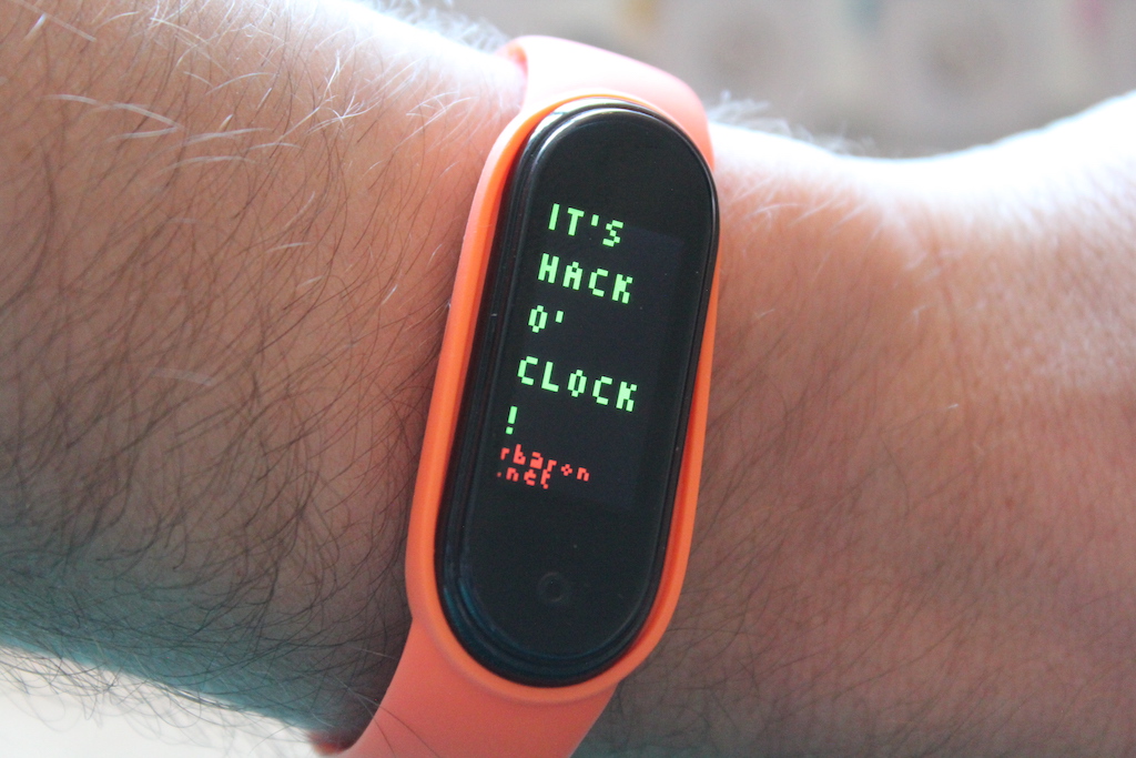
Final Words
If you made it this far, thanks for reading. I hope you enjoyed it. As much as it is a lot of fun, writing posts like this takes a lot of time and effort. If you want to show your support, consider following me on Twitter.