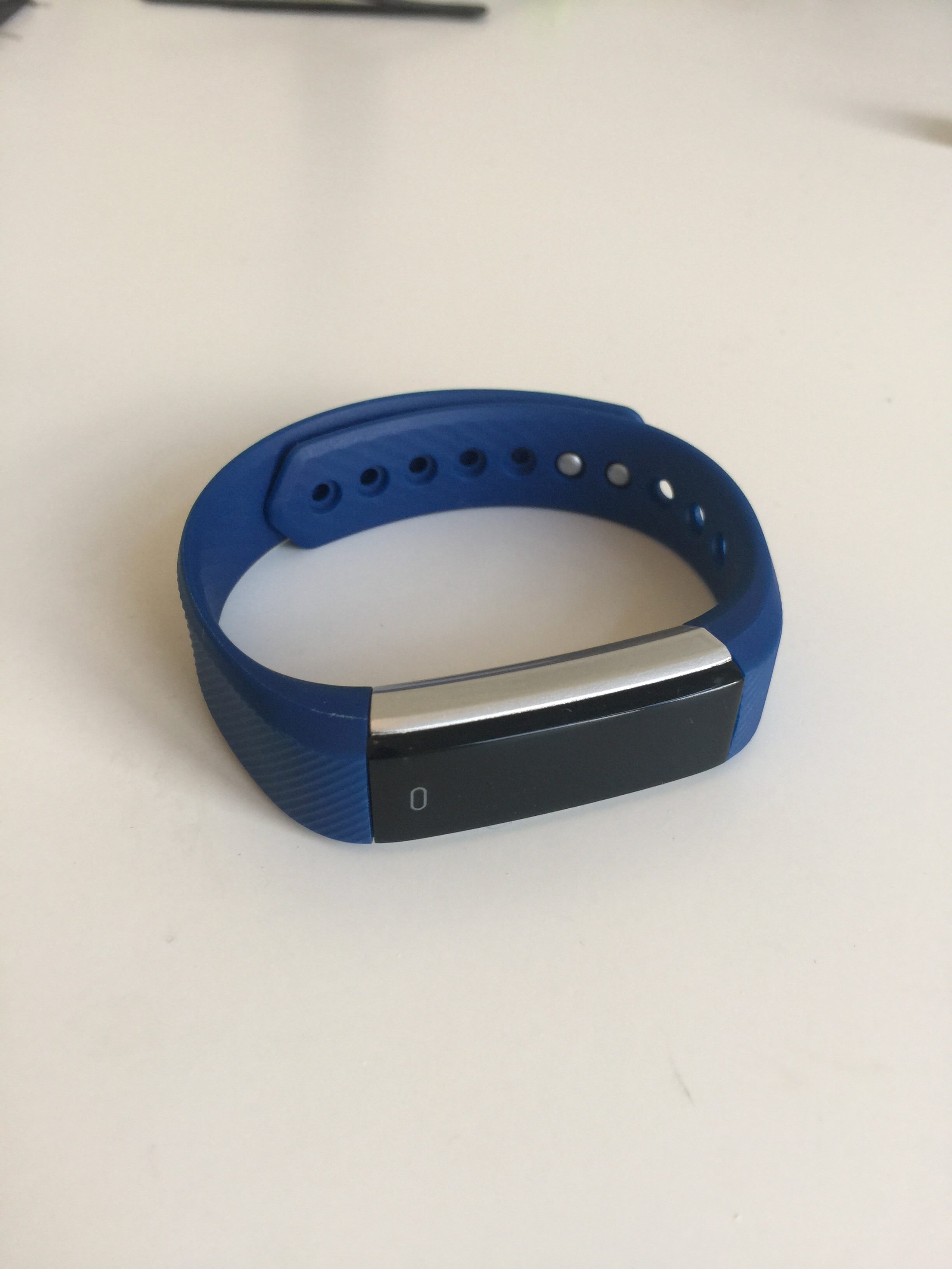
When I joined my current company, I was kindly greeted with a set of goodies on the first day of work. Among these goodies, there was this customized fitness tracker bracelet. Now, orthogonally to one’s fitness inclinations, this is an incredibly cool device from a purely technological standpoint:
- Really small form factor (roughly 15mm x 40mm)
- Bluetooth low energy (BLE)
- OLED display (96x32 pixels)
- Rechargeable battery
- USB charging
- Accelerometer
- Vibration motor
- ~ $10 price point (!)
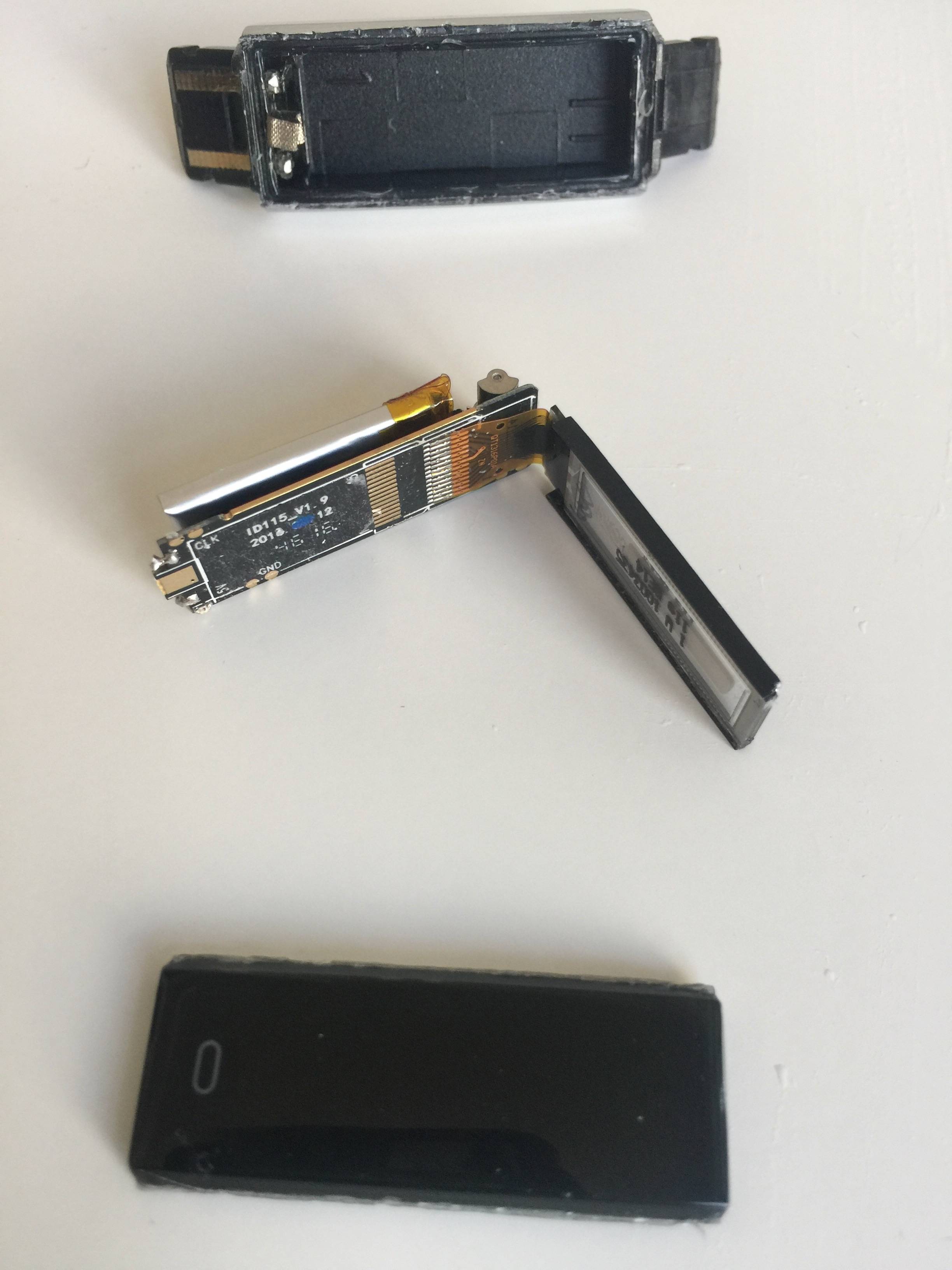
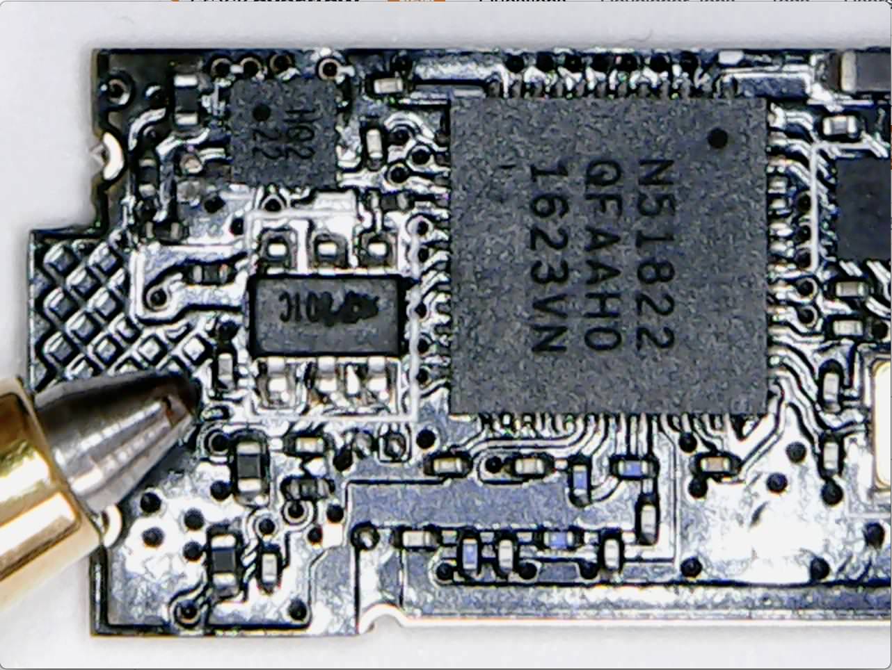
On the outside, on the back, the only identification is a print that says “FCC ID: 2AHFTID115”. Googling it seems to suggest the name of the device is ID115, and there are even a few internal photos of it. In hindsight, on one of these photos, if we try really hard, we can make out the print on the largest integrated circuit (IC) to be “N51822”. This suggests that the microcontroller unit (MCU) might be the Nordic’s nRF51822, a 32-bit ARM M0 CPU with embedded support for Bluetooth low energy, which could, in theory, be reasonably easily programmed to do other things than the bracelet is supposed to do.
Before tearing it down, I did some more googling and found out that some similar bracelets pack the same chip and people have had success in programming it.
Opening it isn’t too easy. The black plastic cover is glued onto the grey plastic back. I used a hair dryer to try and make the glue softer and a small knife to patiently cut through the glue without damaging the plastic too much. After opening it up, I confirmed that it really packs the nRF51822. Later on, I bought a seemingly identical bracelet, but which uses a Texas Instrument MCU. Be aware that variations exist.
Figuring out how to talk to it
On the documentation, it says that the chip can be programmed/debugged using Arm’s Serial Wire Debug (SWD) two-pin interface. This means two things, if we ever wanna talk to it:
- We'll need a "SWD programmer" (of which Segger's J-Link is one)
- We'll need access to the two SWD pins on the MCU, namely SWDIO (data) and SWDCLK (clock)
Luckily, there are some exposed pads on the board. Even though their existence is explained by the need of debugging/testing/verification, I choose to think there’s this cool engineer out there who left these pads there as little gifts for people like us. They’re not all properly labeled, so I suggested some names for them:
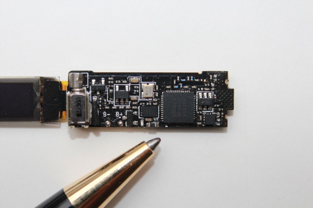
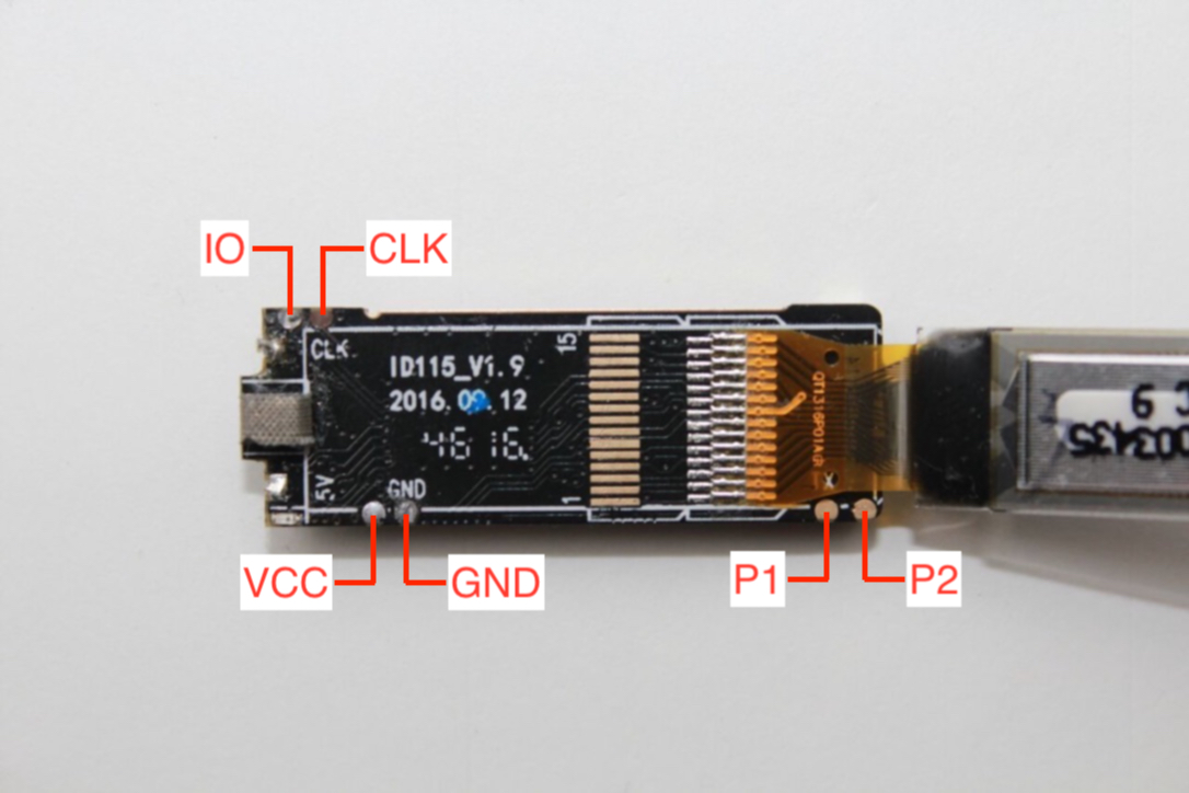
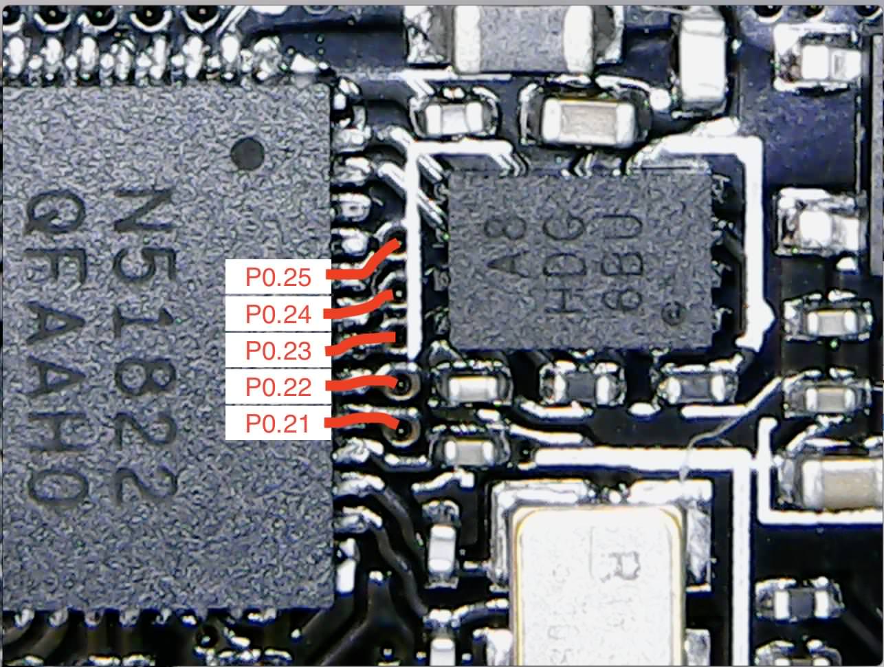
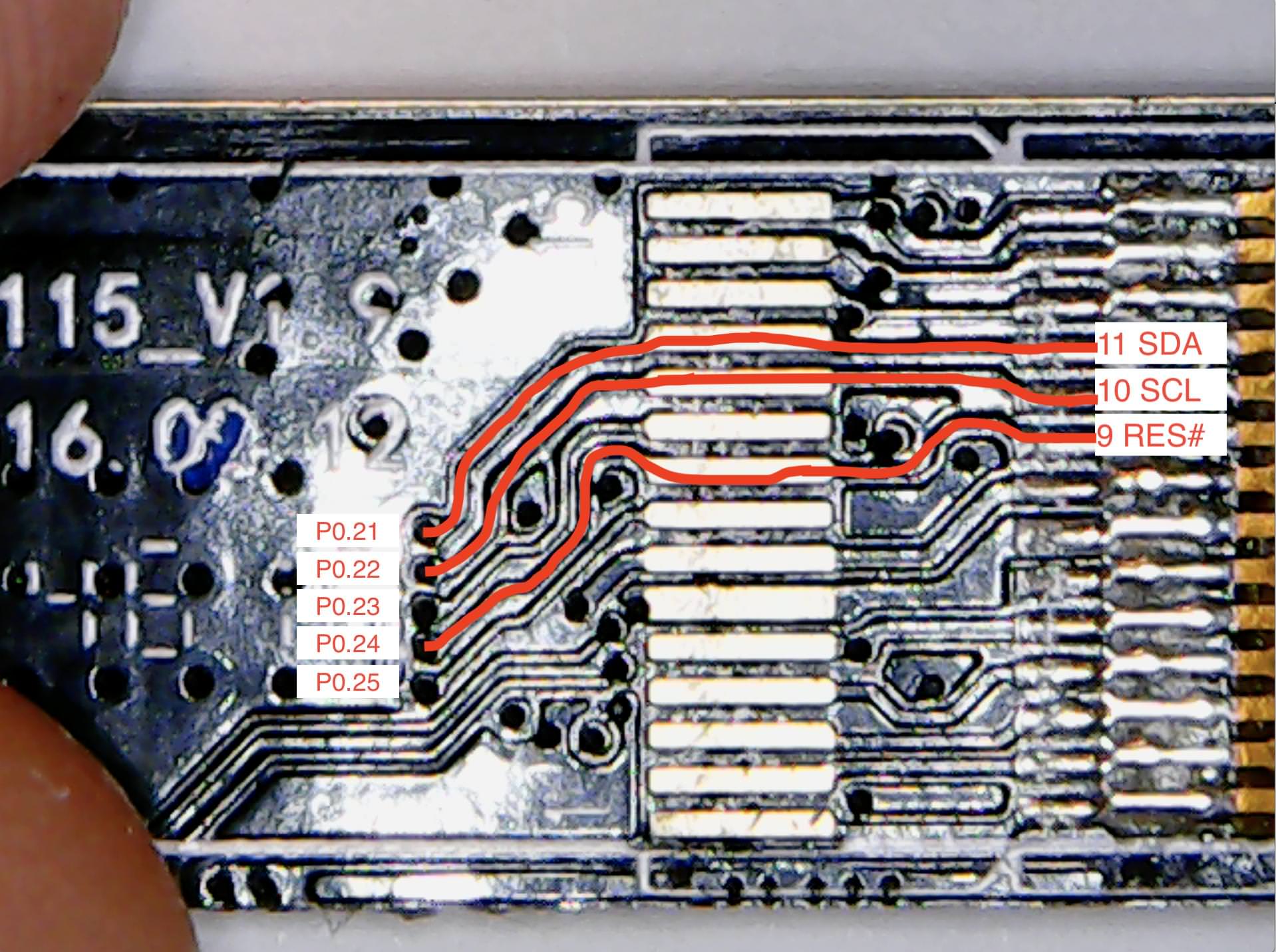
Using an equally cheap USB microscope, I took a few shots of the front and the back of the board and tried to follow the traces from the MCU to the pads.
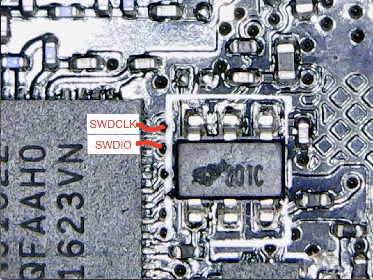
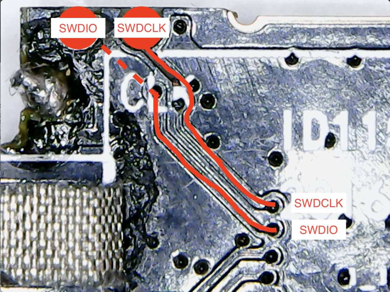
Note that this is a multi-layer PCB and there are through-holes on it, so we need to follow the traces on both sides of the board. Using these images, we can follow the SWDIO and SWDCLK pins from the chip to the IO and CLK pads. This confirms that the label “CLK” on the board is, in fact, the SWDCLK MCU pin, and that the unlabeled one right by it is the CWDIO MCU pin. We can know build our first mapping table:
| nRF51822 Pin | Pad | Description |
|---|---|---|
| SWDIO | IO | Data pin for the SWD programmer |
| SWDCLK | CLK | Clock pin for the SWD programmer |
Open-chip surgery
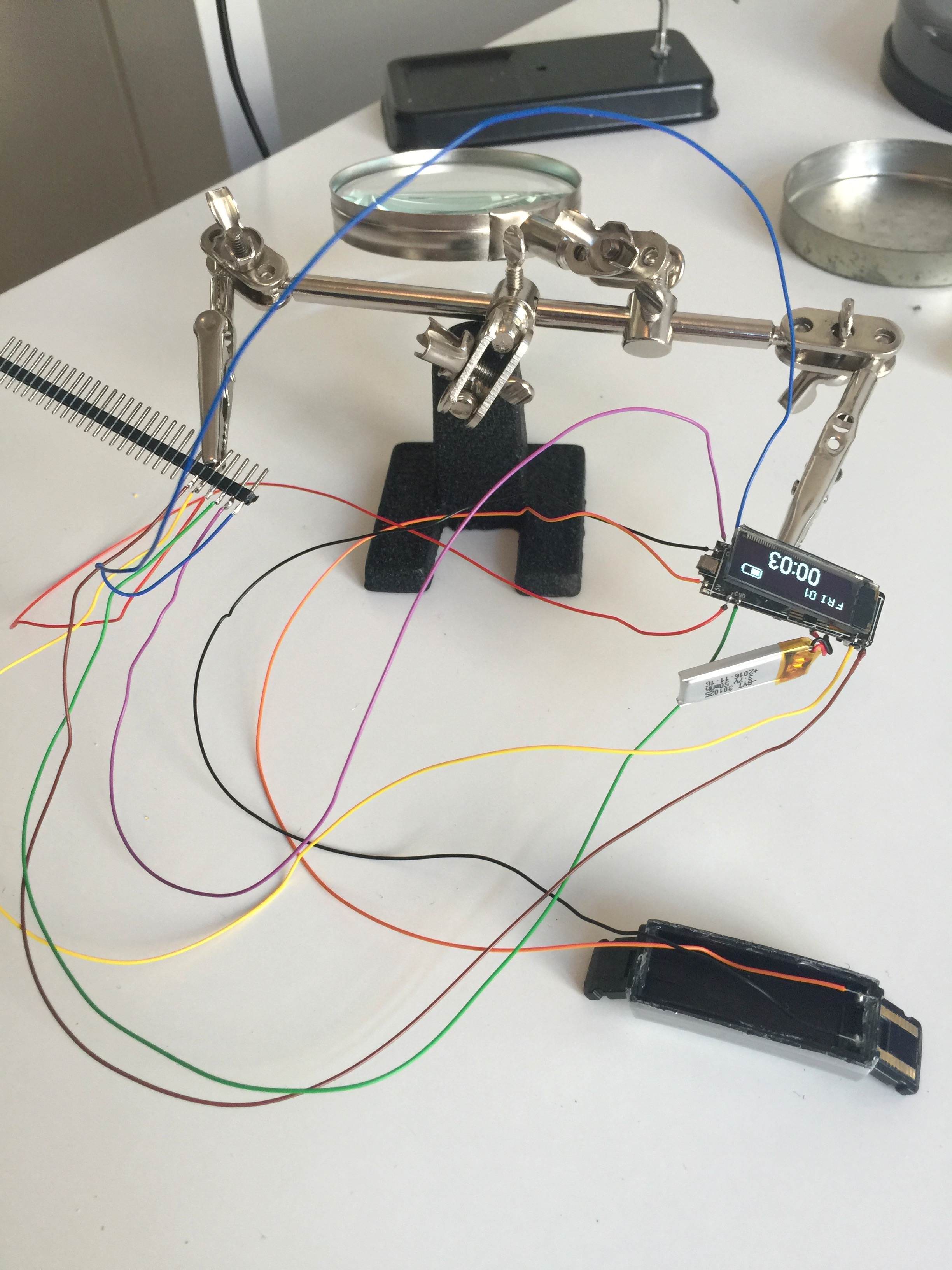
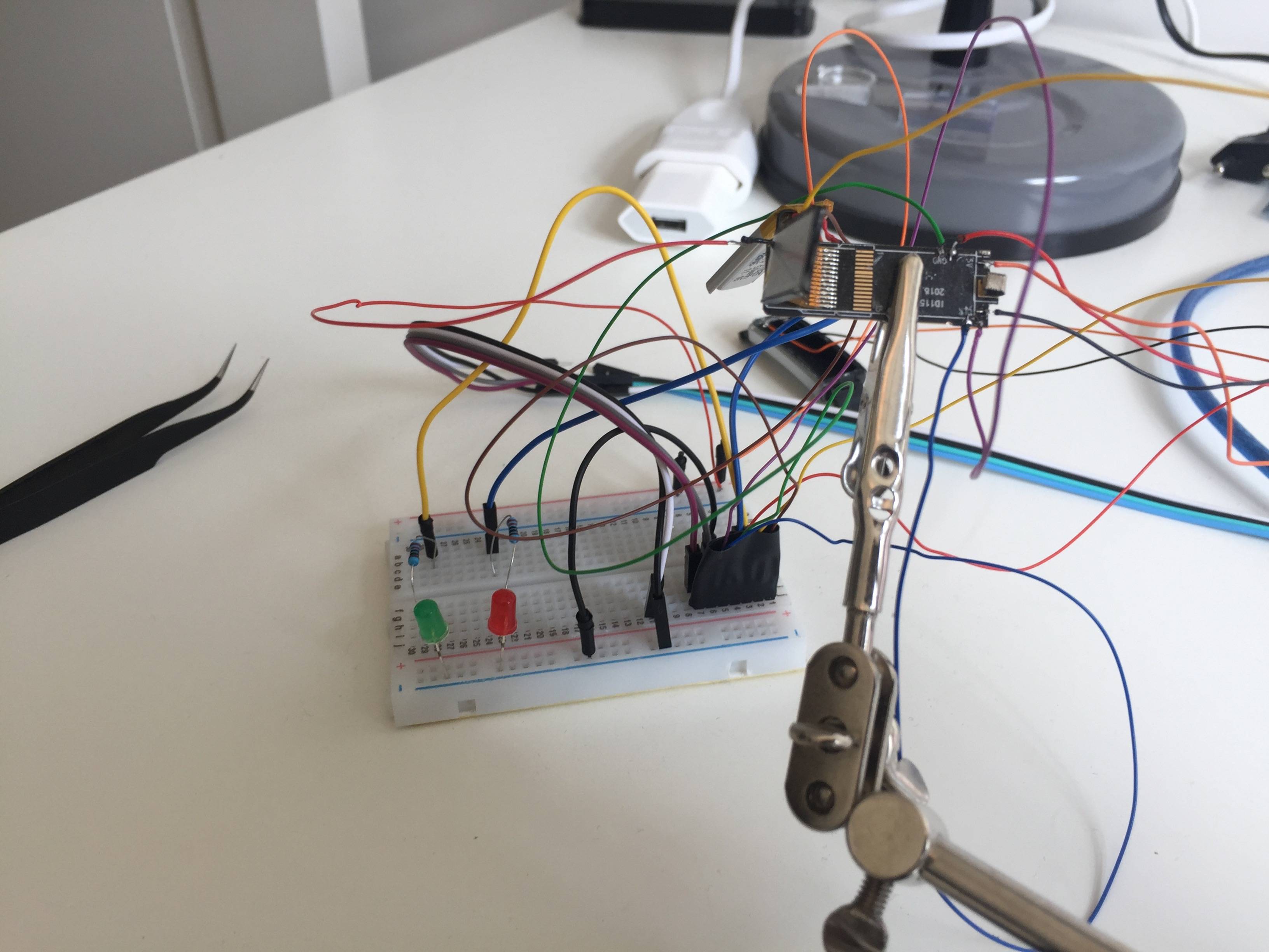
Having access to the two SWD pads, I soldered really thin wires on those pads and on all other exposed pads.
Blinky
The next goal was to try and program the device to do something. In order to run the simplest of the programs on it, we’ll need to make sure:
- We traced the SWDIO/SWDCLK pins correctly
- The SWD programmer works and the computer can talk to it
- We can cross-compile an Arm program and use Nordic's SDK correctly
- We can flash the compiled program into the chip
- Chip is correctly powered and boots our program
The “hello, world” in this case could be a program that turns a LED on and off repeatedly. Even that isn’t too straight-forward, since there’s no build-in LED on the board and if we add an external one, we’ll still need to figure out where to hook it up. This adds another degree of freedom to the problem. By the no-free-lunch theorem, I just hooked two LEDs on the P1 and P2 pads, hoping that we could reach these pads from the MCU.
For the J-Link SWD programmer, drivers and command line programs can be installed from Segger’s website. If you’re on macos and use homebrew, there’s a cask formula in caskroom/drivers/segger-jlink. This will let you talk to the SWD programmer using the JLinkExe command line program.
I then downloaded and extracted Nordic’s nRF5 SDK (I’m using version 12.3.0). Digging through the examples in sdk, it’s clear we will need a compiler that knows how to spit out Arm programs. So I also installed gcc-arm-embedded (also available on homebrew).
Looking around in the SDK and also on Nordic’s development forums, it becomes clear that the SDK is most commonly used with development kits/boards such as this one. The SDK comes pre-configured for a few variations of development kits. Since we’re talking directly to the MCU, we’ll need to tweak some settings on the SDK.
I spent a lot of time understanding the nRF5 ecossystem and getting the program to run on the chip, but it finally worked! You can see the two blinking LEDs on the video above. At this point, I created a Github repo and dumped the working program there with a working Makefile. One of the biggest tricks was figuring out that there are actually a few variants of the nRF51822, and mine had only 16kB of RAM. So I also had to tweak the linker script to take that into account.
Digital IO
As I mentioned, process of getting the LEDs to blink also included hoping and guessing which of the pins in the MCU are connected to P1 and P2, where I had hooked the LEDs. The simplest strategy was to loop through the digital IO pins and repeatedly pull their outputs high and low. To my surprise, both LEDs flashed! To my biggest surprise, the vibration motor also turned on and off!
Doing a manual binary search, I identified the following additional mapping:
| nRF51822 Pin | Pad | Description |
|---|---|---|
| P0.30 | P1 | General purpose digital IO |
| P0.00 | P2 | General purpose digital IO |
| P0.01 | - | Vibration motor |
printf
The ability of talking back to the computer is invaluable when debugging. The J-Link programmer supports Real-Time Transfer (RTT), which can be used to both send and receive data from the chip to a computer. To use it, we need to #include "SEGGER_RTT.h" and call SEGGER_RTT_WriteString(). To read it on the computer, call the jlinkrttlogger CLI, shipped together with the J-Link package.
OLED
Getting the OLED to work was another great challenging task. The most common OLED displays on the market use the ssd1306 driver/controller, and usually talks with the MCU serially, either using SPI or I²C. Here’s an example from Adafruit.
I couldn’t find a similar display on any of the usual shops. 96x32 pixels seems to be a relatively uncommon size, too. Googling the identification number on the display, “QT1316P01A”, the top matches come from chinese websites. The closest one I was able to find was on aliexpress, but there wasn’t any documentation besides the following pin names:
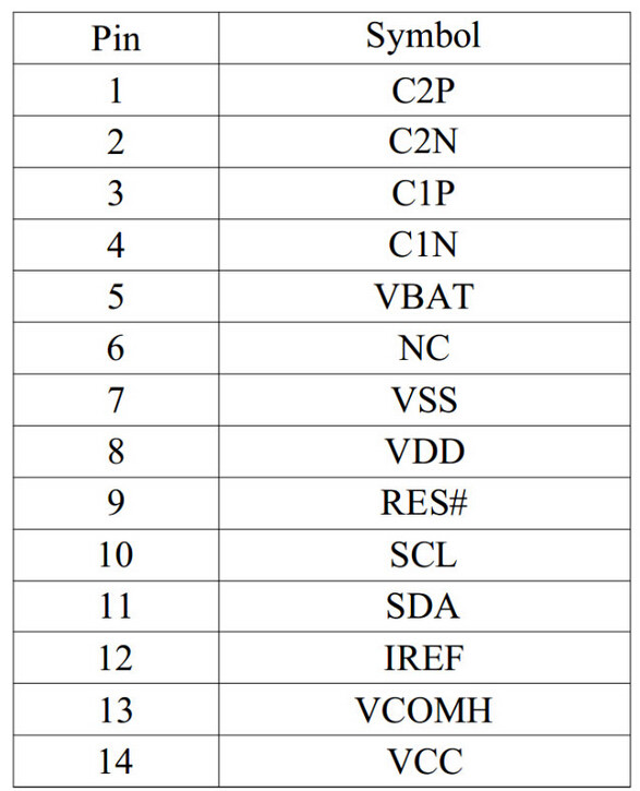
If this documentation is correct, the presence of SCL, SDA, RES# pins indicates that this is a I²C variant. If we can find a reasonable connection between three of the nRF51822 pins and these three OLED pins, it would suggest that we’re on a good track. Back to the microscope.
Tentativelly creating a new mapping table:
| nRF51822 Pin | Pad | Description |
|---|---|---|
| P0.21 | - | OLED SDA pin |
| P0.22 | - | OLED SCL pin |
| P0.24 | - | OLED RES# pin |
The I²C protocol is substantially more involved than, for instance, simple serial protocol like UART. One of the advantages is that it supports multiple masters and multiple slaves on the same bus. This adds a little bit of complexity, because, on the bare minimum, we will need to tell to which slave the MCU should talk. So, on a high level, in addition to the physical pins, there is a “logical” address for the OLED display.
Luckily, one of the examples in the nRF5 SDK is a I²C scanner. In short, it tries to talk to every possible logical address and reports back when there’s something on the other end. My modified version is here. Running it and listening to the logs yields:
$ make
# ...
$ make flash
# ...
$ make log
# ...
TWI scanner.
TWI device detected at 0x3c.
This is great news! We have good reasons to believe the display was correctly identified and it’s really a I²C variant. Googling will tell that 0x3c is a common address for such devices.
We’re now in a good position to try and send some pixels to the display. At this level, there’s no library abstraction. On the ssd1306 documentation we can find the low level approach for pushing data to it. The process consists of a sequence of configuration commands that, among other things, sets the display orientation, writing mode and size. After these, a sequence of data bytes are sent to the displays’s graphic display data RAM (GDDRAM), which are mapped onto the screen.
In order to get the configuration right, I took a look under the Adafruit’s ssd1306 library’s hood and tried to emulate similar commands. This is where I spent most of the time in this project. Getting all the details right was very time consuming, and there are still behaviors I cannot explain. Nevertheless, it works!
Code for this example is here.
With these settings, the display is divided in 4 rows (pages) of 96 columns. So pages are 8 pixels high. The first byte sent will be laid down “vertically” on the first column of the first page. The second byte will occupy the second column, then the third and so on, until the 96th column, when it will wrap around and begin at the first column on the second page.
Or rather, that is the expected behavior. As it’s apparent in the video below, the observed behavior is different: the odd columns are filled in first, then the even columns and only then it wraps around.
I spent a lot of time to figure out this was the reason I was seeing nonsense on the display, and then some more time tweaking the configuration to try and fix this. In the end, I swallowed my pride and implemented this weird rendering logic as part of the program and called it a day.
Trip to Arduino land
During the time I spent digging through Adafruit’s ssd1306 library for Arduino, I wished there was a way to “mock” the Arduino-specific bits and test it on the nRF51822. As it turned out, people much more skilled than me already thought something similar – the amazing sandeepmistry/arduino-nRF5 project does just that. It implements the core Arduino libraries using the nRF5 SDK.
Using this project, we can open the Arduino IDE, select the nRF5 board we want to program and we can leverage lots of the existing Arduino ecossystem. I forked the project and added support for the our bracelet board. It can be selected on the Tools > Board > ID115 Fitness Bracelet (nRF51822) drop-down menu.
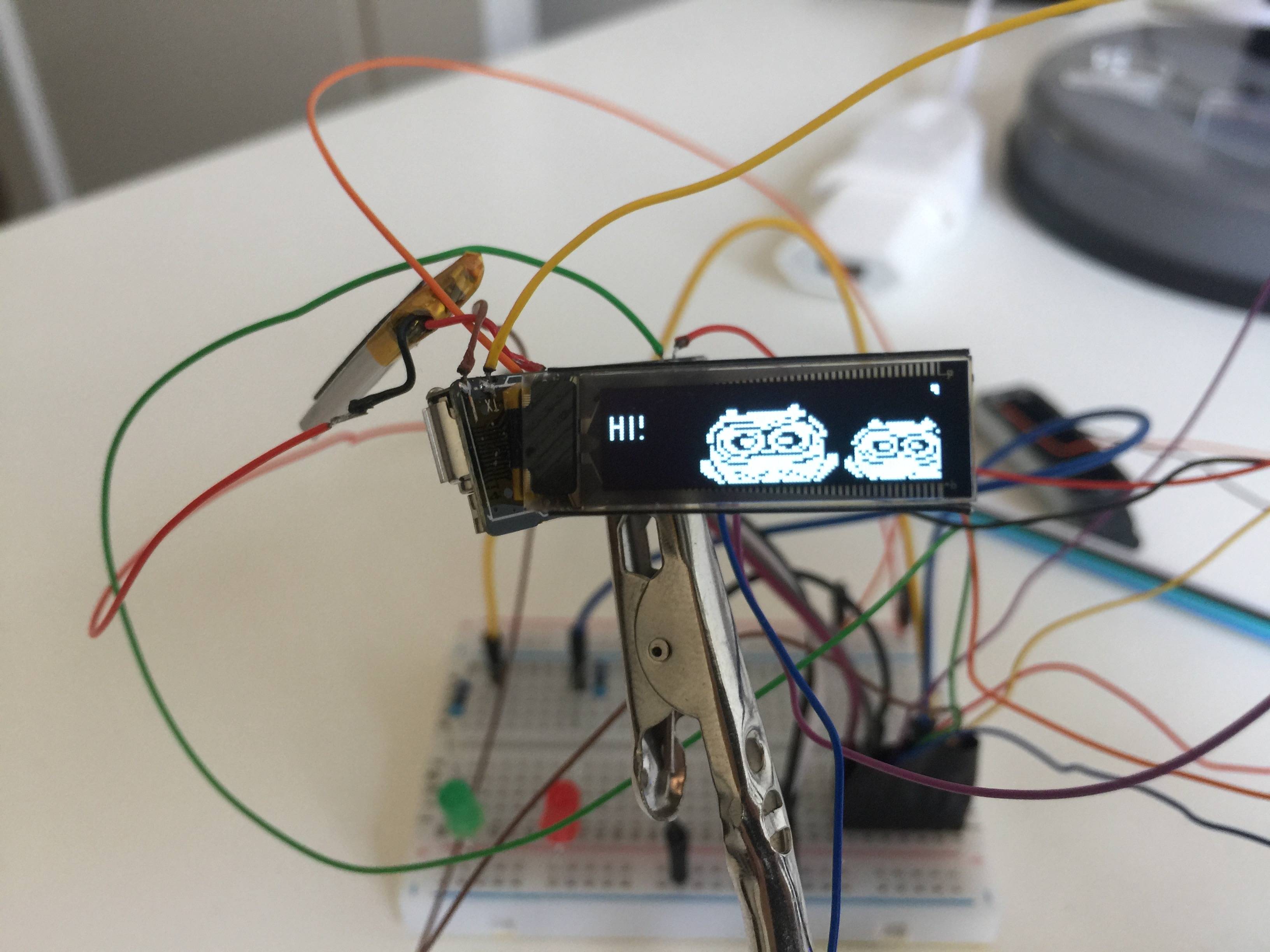
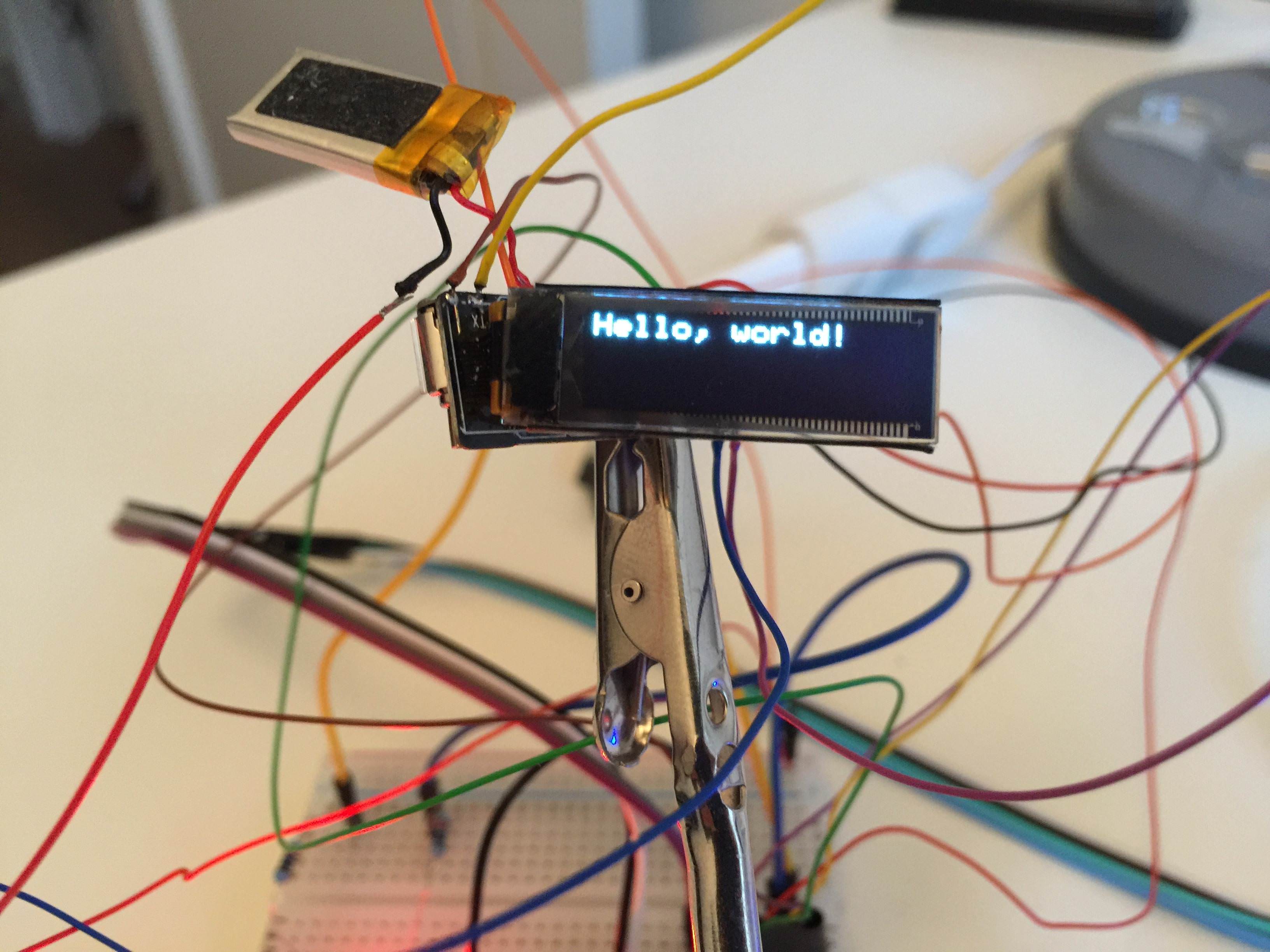
This also means now we can use Adafruit’s OLED library. To my surprise and relief, the same weird “odd-first, then even” OLED behavior happened! I happily forked the library and implemented the same hacky work-around. Now we also get all sorts of nice abstractions over the low-level previous approach, such as drawing text:
Analog IO
In addition to digital, “on/off”, inputs, the nRF51822 also has 10 pins that can read analog inputs. This is useful, for instance, for reading the current battery charge. From the docs, reading from analog pins will yield a 10-bit value, so if the input is at 0V, we’ll read 0, and if it input is at VCC we’ll read 1023, with interpolated values inbetween.
I periodically printed the values of the analog inputs and plotted the most intesting signals results:
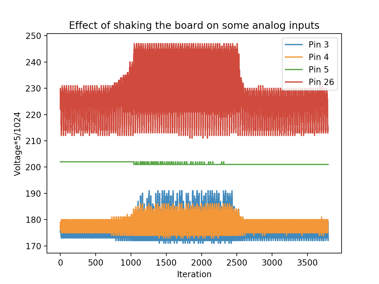
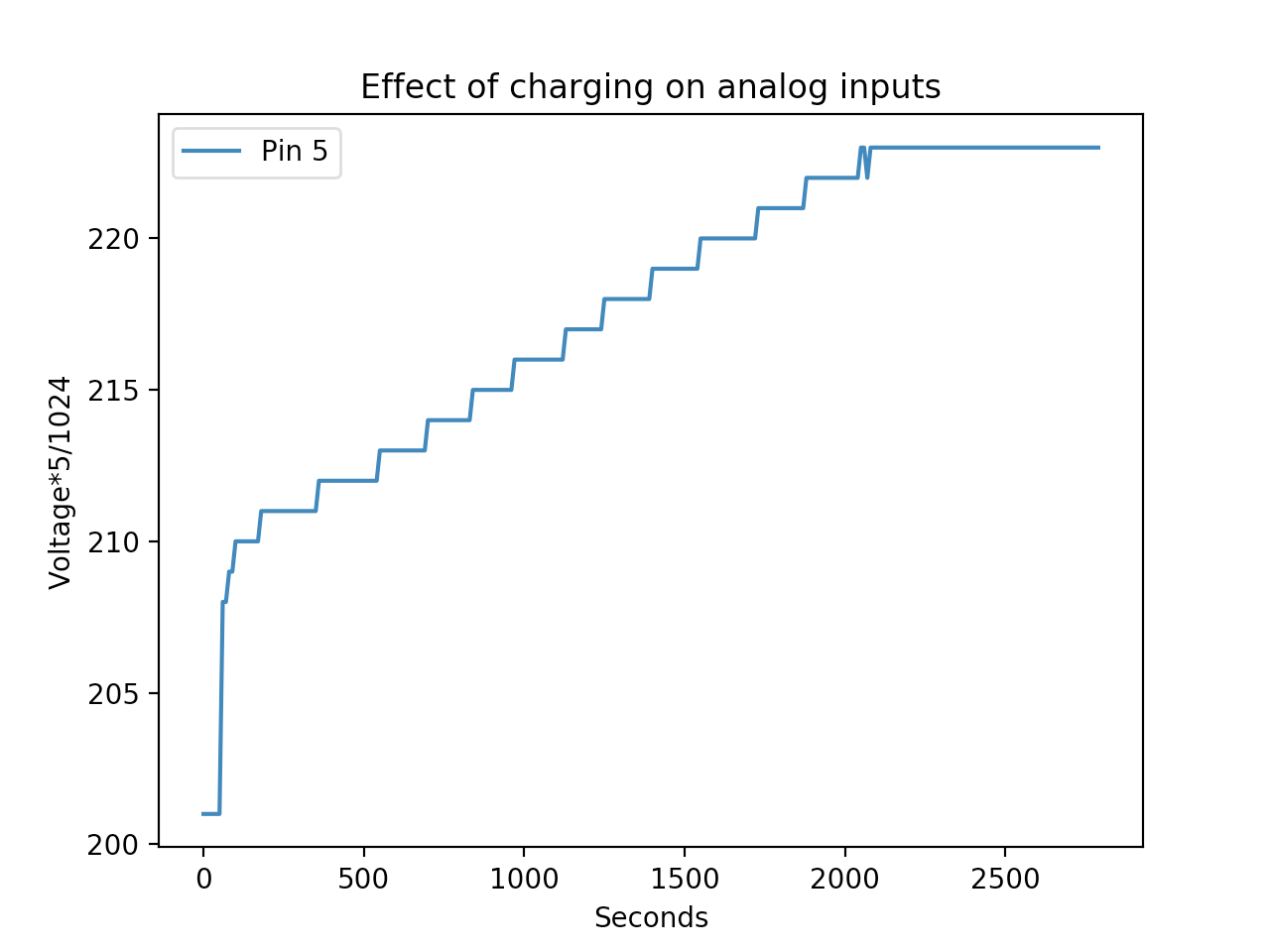
I’m convinced that the pin P0.05 is related to the battery charge state, since it goes up when charging and down when discharging. I suspect that the pin P0.26 is connected to one of accelerometer outputs, since it goes crazy when I shake the board. Pins P0.03 and P0.04 could also be connected to different accelerometer outputs, but this behavior could also be a second order effect on the chip’s inputs. For example, note that on the fist plot how the battery charge level (pin 5) also jiggles when the accelerometer demands more energy. This is an example of a second order effect.
The code can be found on this sketch. The raw data and plotting script is here. We can now add a few lines to our mapping table:
| nRF51822 Pin | Pad | Description |
|---|---|---|
| P0.05 | - | Analog input - Battery charge related |
| P0.26 | - | Analog input - One accelerometer axis |
| P0.03 | - | Analog input - One accelerometer axis (probably maybe) |
| P0.04 | - | Analog input - One accelerometer axis (probably maybe) |
Button
On the original firmware, touching the bracelet’s screen on a specific point makes the screen turn on. Holding it down starts a chronometer, if I remember correctly. This is not a physical clicky button, but some sort of capacitive sensor thingy, which works surprisingly well. Using a similar approach to finding the digital outputs, I found where it’s connected to the MCU:
The code can be found here.
| nRF51822 Pin | Pad | Description |
|---|---|---|
| P0.10 | - | Digital input - Built-in button |
Bluetooth low energy (BLE)
The BLE functionality on nRF5 chips is implemented via something called SoftDevice. This is a pre-compiled binary that contains the BLE stack. It should be flashed independently of the application. There are multiple SoftDevice versions and finding the right one depends both on the SDK version and the chip revision.
There is a compatibility matrix on the documentation (which unfortunatelly is not directly linkable) that shows which chip revision goes with which SDK and which SoftDevice version. In our case, the print on the chip reads QFAAH0, which has 256 kB flash, 16 kB RAM and is compatible with SoftDevice s130.
The SDK version 12.3, which I’ve been using, already packs some examples using this SoftDevice s130. In comparison to the programs we’ve been flashing so far, which are straight-forwardly flashed to the chips 0x0 address, now we will have to flash the SoftDevice to the address 0x0, and the actual program to the address 0x1b000. After booting and initialization, the SoftDevice binary will jump to this adress and hand over control to our program. To illustrate this, I added the same blinky example, but one that starts with the SoftDevice here. The observed behavior is the same, except we need to make sure the SoftDevice is flashed beforehand:
$ make
# ...
$ make flash-softdevice
# ...
$ make flash
# ...
$ make log
# ...
Hello, world!
Arguably, the simplest “hello, world”-type of bluetooth application is such that turns the device into a beacon. The device only broadcasts its presence and it’s the listeners’ duty to do something when they come in range. The SDK ships one of such examples under the same ble_app_beacon. It assumes the SoftDevice s130 has been flashed previously.
Here, too, the fact that we’re talking to the chip directly, instead of through a development kit, made things a lot harder. Besides having to adjust the RAM size (as I sorely learned from the blinky example), there was another hard to track issue. As it turns out, the BLE stack uses an oscillator in order to do timing-sensitive tasks. The SDK examples assumed an external crystal oscillator. Once I figured this out with the power of a thousand printfs, changing the configuration flag to use the synthetic clock generator instead fixed the problem. The beacon source code can be found here.
BLE + Arduino
Once the BLE example was working with the nRF5 SDK, and knowing about the RAM and the oscillator traps, I looked once again into the Arduino environment. And once again, there it was, the glorious sandeepmistry/arduino-BLEPeripheral project (by the same guy as the arduino-nRF5!), which provides a nice abstraction on top of the inner details of setting up a BLE peripheral.
To my surprise, I didn’t even have to fork this library. The author of the arduino-nrf5 project took the time to make all the boards and settings configurable, so choosing the right SoftDevice and oscillator source was as easy as selecting it from the Tools > Low Frequency Clock > Synthesized drop-down menu. Awesome. I set up a quick-and-dirty example on how to use this to turn a LED on/off, as you can see on the video.
Next steps
At this point, after staring at this board for uncountable hours over the span of several weeks, I look very much forward to rellocate it all the way to the back of my drawer and leave it there for some time.